Interconnect structure improvements

a technology of interconnections and structures, applied in the field ofsemiconductor devices, can solve the problems of increasing the stress on the dielectric layer, cracking or damage of low-k dielectric materials, and mechanical weakening of the insulation material, and achieve the effect of high conductivity

Inactive Publication Date: 2005-11-01
INTELLECTUAL DISCOVERY INC
View PDF10 Cites 45 Cited by
  • Summary
  • Abstract
  • Description
  • Claims
  • Application Information

AI Technical Summary

Benefits of technology

[0020]In forming the substantially cylindrical trench opening, a third intermetal dielectric layer may be provided over the second intermetal dielectric layer. In so doing, the second intermetal dielectric layer selectively etches faster than the first and third intermetal dielectric layers so that the etch front partially undercuts bottom comer portions of the second intermetal dielectric layer for forming the substantially cylindrical trench opening. This may be accomplished by varying dopant concentrations of these intermetal dielectric layers, or providing porous intermetal dielectric layers having varying amounts of porosity. Alternatively, the at least second dielectric layer may be a graded dielectric layer having at least one constituent element thereof varied in concentration in a manner that allows the graded dielectric layer etch slowest at a top surface and fastest at a bottom surface thereof for forming the substantially cylindrical trench opening.
[0021]In yet another aspect, the invention is directed to a conductive interconnect structure for preventing cracks in a dielectric layer on a substrate. The conductive interconnect structure includes at least a first intermetal dielectric layer and a substantially cylindrical trench opening therein. The substantially cylindrical trench opening is filled with a high conductivity metal such that a substantially cylindrical wire is formed in the at least first intermetal dielectric layer. This substantially cylindrical wire substantially avoids any propagation points for starting cracks in the at least first intermetal dielectric layer. The conductive interconnect structure may also include at least a second intermetal dielectric layer, whereby the substantially cylindrical wire resides in both the first and the at least second intermetal dielectric layers.

Problems solved by technology

However, as the dielectric constant (low-k) of the material is lowered, the insulator material becomes mechanically weaker, and as such, it becomes significantly easier to crack or damage these low-k dielectric materials.
The presence of device interconnects, such as filled vias and / or rectangular trenches within the low-k dielectric layers, further increase stresses on the dielectric layer, which in turn, increase its susceptibility to cracking and damage.
For instance, during sintering, stresses are primarily built up in the dielectric layer during the cool down cycle, whereby the dielectric layer is put into tension near any metal feature, making it prone to failure by cracking.
That is, the capacitively coupled noise between neighboring rectangular shaped lines will become very severe.
In addition, when the upper trench comers are rounded concave downward, the occurrence of undesired wire shorts between adjacent trenches increases, due to residual metal, which degrades the IC yield and / or reliability.
Each of these rectangular parallelepipeds have at least one sharp corner and / or a flat edge, and as such, suffer from the above problems of propagation and nucleation points for potential cracks within the dielectric layer 10, as well as increased capacitively coupled noise between neighboring rectangular parallelepiped conductors.

Method used


Image

  • Interconnect structure improvements
  • Interconnect structure improvements
  • Interconnect structure improvements

Examples


Embodiment Construction

[0029]In describing the preferred embodiment of the present invention, reference will be made herein to FIGS. 3A–5C of the drawings in which like numerals refer to like features of the invention.

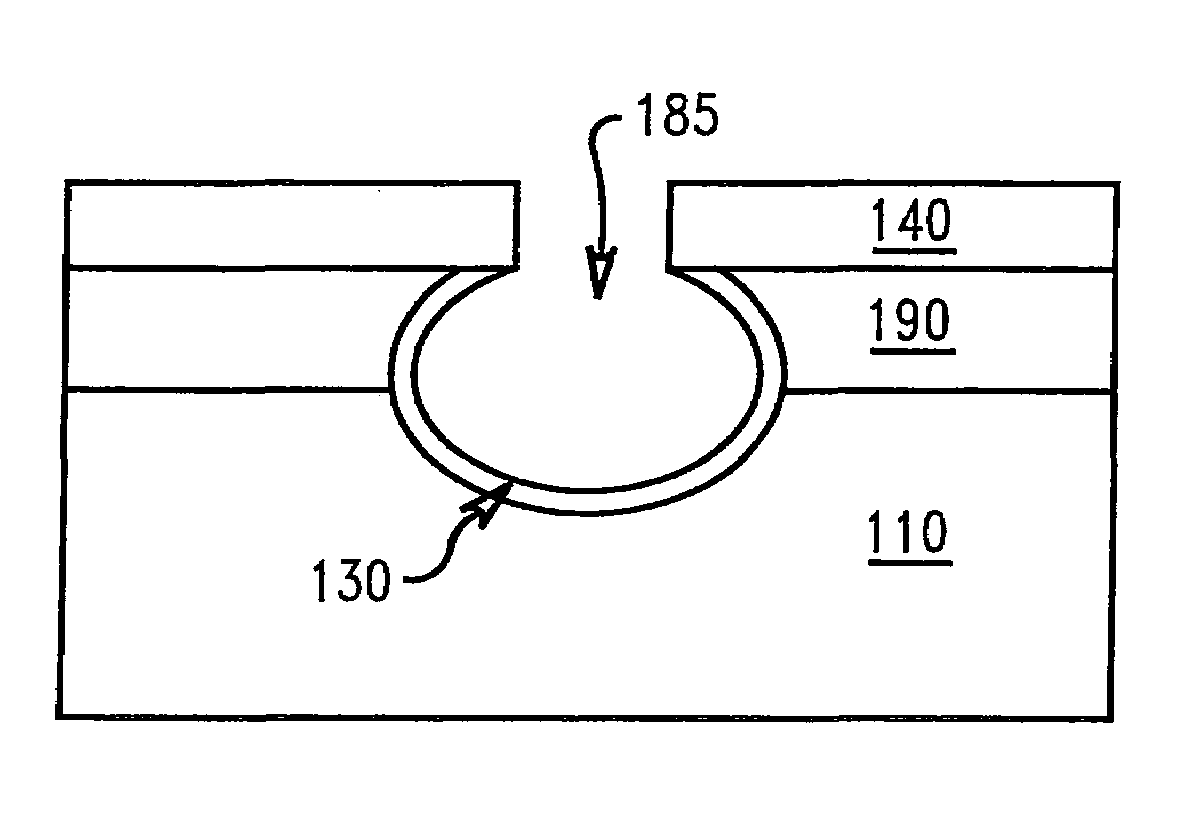
[0030]The present invention provides methods of forming and the interconnect structures (IC) formed having half cylindrical, substantially cylindrical, or cylindrical conductors, preferably wires. These half cylindrical, substantially cylindrical, or cylindrical wires advantageously reduce the line-to-line capacitance between neighboring conductors, reduce mechanical stresses induced on the IC, and as such, increase the overall mechanical strength of the IC. It should be appreciated that the wires of the present invention, with half cylindrical or cylindrical cross-sectional shapes, are understood to be nearly or approximately shaped as described and not ideal geometric half cylinders or cylinders.

[0031]As the conductors of the invention are formed with half cylindrical, substantially cylind...


PUM


Abstract

Methods and conductive interconnect structures are provided for preventing cracks in a dielectric layer on a substrate. Substantially half cylindrical or cylindrical trench openings are formed within at least one dielectric layer, which are then filled with a high conductivity metal for forming substantially half cylindrical or cylindrical wires. The rounded bottom portions of the substantially half cylindrical wires, or the rounded bottom and top portions of the substantially half cylindrical wires, avoid any propagation points for starting cracks in the dielectric layer, as compared to conventional rectangular conductors having angled edges, which in fact are propagation points for initiating cracks. The substantially half cylindrical or cylindrical wires also reduce the line-to-line capacitance between neighboring wires, substantially eliminate any high stress points in the dielectric layer, reduce mechanical stresses induced on the IC and increase the overall mechanical strength of the IC.

Description

BACKGROUND OF INVENTION[0001]The present invention relates to semiconductor devices, and more particularly, to methods of forming and the resultant structures formed having cylindrical or substantially cylindrical wires for reducing both induced mechanical stresses on the structure and the line-to-line capacitance.[0002]Integrated circuits (ICs) are fabricated by building multiple layers of wiring and passivation on substrates (wafers) that contain semiconductor devices. Often, interconnect metal conductive layers are connected to each other, and to the substrate, by patterned insulative layers residing over and under such interconnect metal conductive layers. These insulative layers are commonly composed of a dielectric material. The openings, such as trenches and vias, are etched into the insulative layers, by damascene or dual damascene processing, in locations where conductive wires or contacts are desired between conductive regions. These conductive regions may include previous...

Claims


Application Information

Patent Timeline
Patent Type & Authority Patents(United States)
IPC IPC(8): H01L21/02H01L21/44H01L21/768H01L23/528H01L23/532
CPCH01L21/76804H01L21/76877H01L23/5283H01L23/53238H01L2924/0002H01L2924/00
Inventor DALTON, TIMOTHY J.FITZSIMMONS, JOHN A.GAMBINO, JEFFREY P.NICHOLSON, LEE M.SIMON, ANDREW H.STAMPER, ANTHONY K.
Owner INTELLECTUAL DISCOVERY INC
Why Eureka
Try Eureka