Process to manufacture nonvolatile MOS memory device

a technology of nonvolatile mos and memory devices, which is applied in the field of microelectronics, can solve the problems of long processing time, uniform germanium profile in the oxide, and limitations of ion implantation technique, and achieve the effects of improving quality, improving control of oxide and interface quality, and improving quality

Inactive Publication Date: 2005-11-08
CHARTERED SEMICONDUCTOR MANUFACTURING
View PDF8 Cites 10 Cited by
  • Summary
  • Abstract
  • Description
  • Claims
  • Application Information

AI Technical Summary

Benefits of technology

[0011]These objects have been achieved by initial use of rapid thermal oxidation to grow a high quality layer of thin tunnel oxide. Chemical vapor deposition is then carried out to deposit a germanium doped oxide layer. A capping oxide is then deposited following which the structure is rapid thermally annealed to synthesize the germanium nanocrystals. The use of chemical vapor deposition process does not place a lower limit on the top control-oxide thickness. It also gives rise to better control oxide and interface quality as ion implantation damage is absent. In addition, the oxide in which the germanium nanocrystals are embedded is of better quality as compared to a sputtered oxide. This results in superior charge retention capability.

Problems solved by technology

However, the ion implantation technique has its limitations such as a long processing time, a non-uniform germanium profile in the oxide and a compromise on the control oxide and interface quality.
However, the subsequent sputtering step results in a non-stoichiometric oxide film and also has a problem with particle generation.

Method used


Image

  • Process to manufacture nonvolatile MOS memory device
  • Process to manufacture nonvolatile MOS memory device
  • Process to manufacture nonvolatile MOS memory device

Examples


Embodiment Construction

[0018]Overview: Rapid thermal oxidation is first used to grow a high quality layer of thin tunnel oxide. Chemical vapor deposition is then carried out to deposit a germanium doped oxide layer. A capping oxide is then deposited following which the structure is rapid thermally annealed to synthesize the germanium nanocrystals.

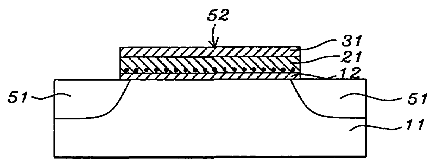
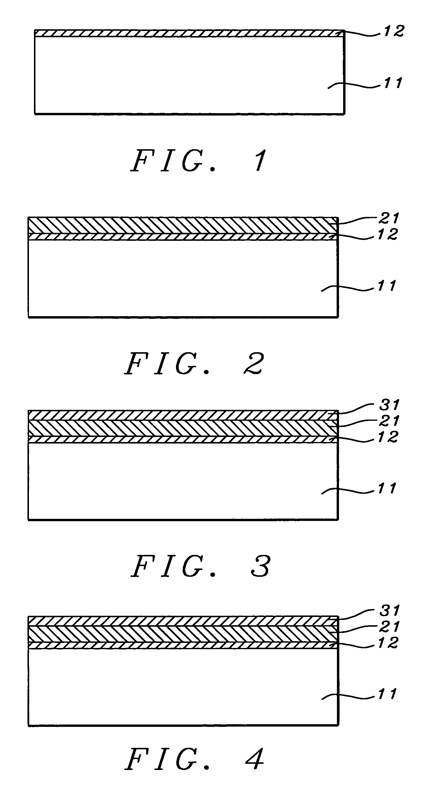
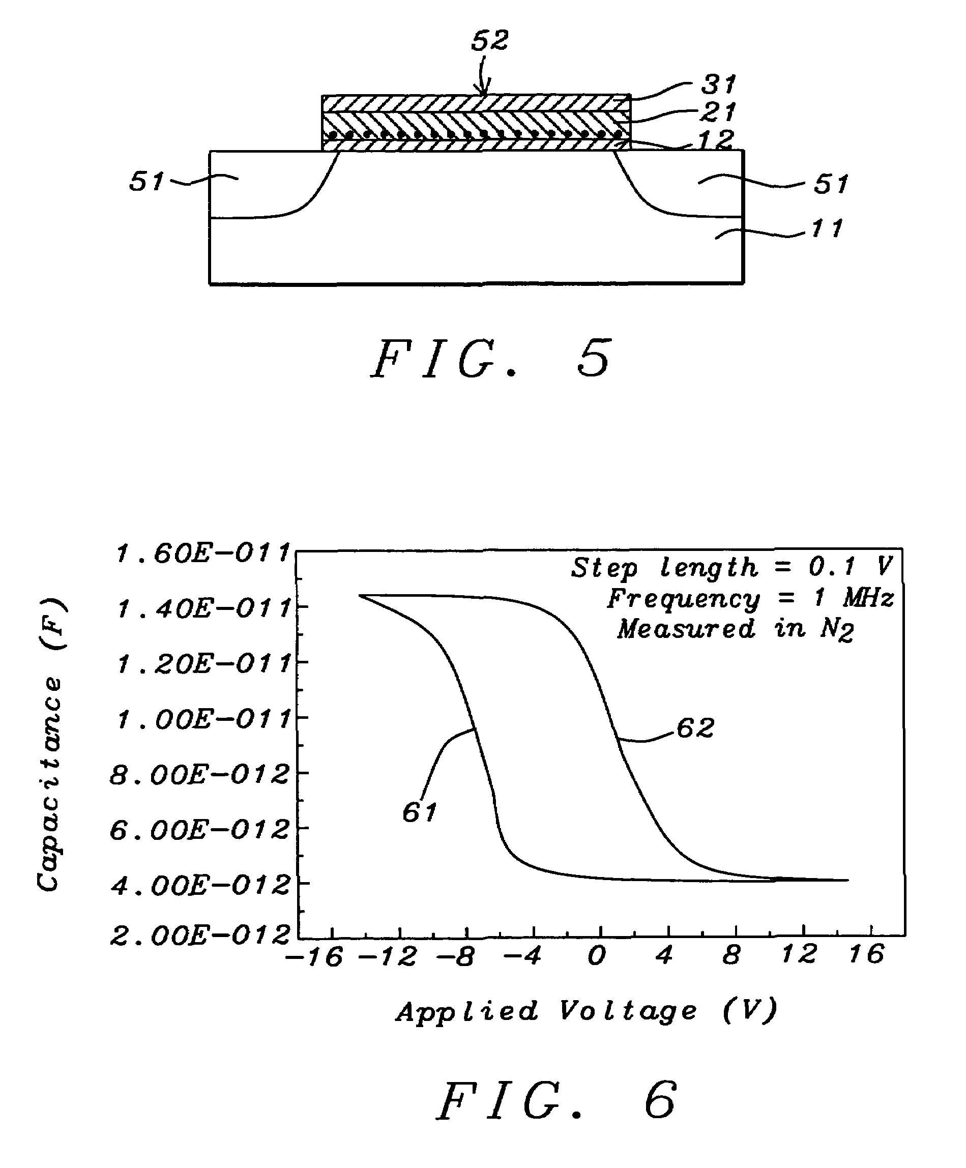
[0019]Referring now to FIG. 1, the process of the present invention begins with the provision of silicon body 11. Body 11 is preferably P-type but this is not essential for the invention to work. Tunnel oxide layer 12 is then grown on the upper surface of 11. This was achieved by means of rapid thermal oxidation (at between about 900 and 1,000° C. for between about 5 and 60 seconds in a dry oxygen ambient), leading to an oxide thickness that is between about and 2 and 5 nm.

[0020]Next, as seen in FIG. 2, layer 21 of germanium doped silicon dioxide is deposited onto tunnel oxide layer 12. Layer 21 was formed by reacting silane in a mixture containing between about ...


PUM

PropertyMeasurementUnit
thicknessaaaaaaaaaa
thicknessaaaaaaaaaa
thicknessaaaaaaaaaa

Abstract

Devices with embedded silicon or germanium nanocrystals, fabricated using ion implantation, exhibit superior data-retention characteristics relative to conventional floating-gate devices. However, the prior art use of ion implantation for their manufacture introduces several problems. These have been overcome by initial use of rapid thermal oxidation to grow a high quality layer of thin tunnel oxide. Chemical vapor deposition is then used to deposit a germanium doped oxide layer. A capping oxide is then deposited following which the structure is rapid thermally annealed to synthesize the germanium nanocrystals.

Description

FIELD OF THE INVENTION[0001]The invention relates to the general field of microelectronics with particular reference to nonvolatile MOS devices, more specifically to their manufacture.BACKGROUND OF THE INVENTION[0002]In the upcoming age of nanotechnology, where devices may be a thousand times smaller than the microchips of today, semiconductor nanocrystals (Quantum Dots) have exhibited charge storage capability. This promises to be useful in future non-volatile memory applications and is currently under investigation by various research groups.[0003]Charge storage devices that exceed the performance limits of a conventional floating-gate device have attracted a great deal of interest and are spurring rapid progress in this area. Quasi-nonvolatile MOS memory devices employing silicon nanocrystal charge-storage sites produced by ion implantation into the gate oxide have already been demonstrated (Tiwari et al., Appl. Phys. Lett. 68 (10), p.1377, 1996) or germanium (King et al. IEDM Te...

Claims


Application Information

Patent Timeline
Patent Type & Authority Patents(United States)
IPC IPC(8): H01L21/336H01L21/02H01L21/70H01L21/8242H01L21/28H01L29/423H01L29/788
CPCB82Y10/00H01L21/28282H01L29/42332H01L29/7881Y10S438/962H01L29/40117
Inventor HO, VINCENTCHOI, WEE KIONGCHAN, LAPCHIM, WAI KINNG, VIVIANHENG, CHENG LINTEO, LEE WEE
Owner CHARTERED SEMICONDUCTOR MANUFACTURING
Why Eureka
Try Eureka