Method for forming a low-k dielectric layer for a semiconductor device

a semiconductor device and dielectric layer technology, applied in the direction of coatings, metallic material coating processes, chemical vapor deposition coatings, etc., can solve the problems of poor oxidation resistance and propagation delay, and achieve excellent reactive ion etching characteristics, excellent step coverage and uniform thickness, and low etching rate

Inactive Publication Date: 2005-11-08
SAMSUNG ELECTRONICS CO LTD
View PDF5 Cites 76 Cited by
  • Summary
  • Abstract
  • Description
  • Claims
  • Application Information

AI Technical Summary

Benefits of technology

[0012]It is another feature of an embodiment of the present invention to provide a method for forming a SiBN dielectric layer having excellent step coverage and uniformity in thickness over an entire surface of a wafer using an atomic layer deposition (ALD) process.
[0014]It is yet another feature of an embodiment of the present invention to provide a method for forming a SiBN dielectric layer having an excellent reactive ion etching (RIE) characteristic.
[0020]The third reactive material may be NH3 or N2H4 gas and may be supplied at a gas flow rate of 500 sccm. The third reactive material may be N2, H2 and NH3 gases and a mixture of these gases with a radical type. The third reactive material may be converted to plasma in the chamber by using an inductive coupled plasma (ICP) generation process, a direct current (DC) plasma generation process, a radio frequency (RF) plasma generation process or a microwave plasma generation process to increase a reaction rate between the first and second reactive materials and the third reactive material.

Problems solved by technology

This high dielectric constant causes a propagation delay since parasitic capacitance increases as a chip size is reduced.
For example, an ALD BN layer is easily hydrolyzed by moisture in the atmosphere, is wet etched by a high temperature wet chemical based on sulfuric acid H2SO4, and has poor oxidation resistance.

Method used


Image

  • Method for forming a low-k dielectric layer for a semiconductor device
  • Method for forming a low-k dielectric layer for a semiconductor device
  • Method for forming a low-k dielectric layer for a semiconductor device

Examples


Embodiment Construction

[0031]Korean Patent Application No. 2002-11671, filed on Mar. 5, 2002, and entitled: “Method for Forming Thin Layer Using ALD,” is incorporated by reference herein in its entirety.

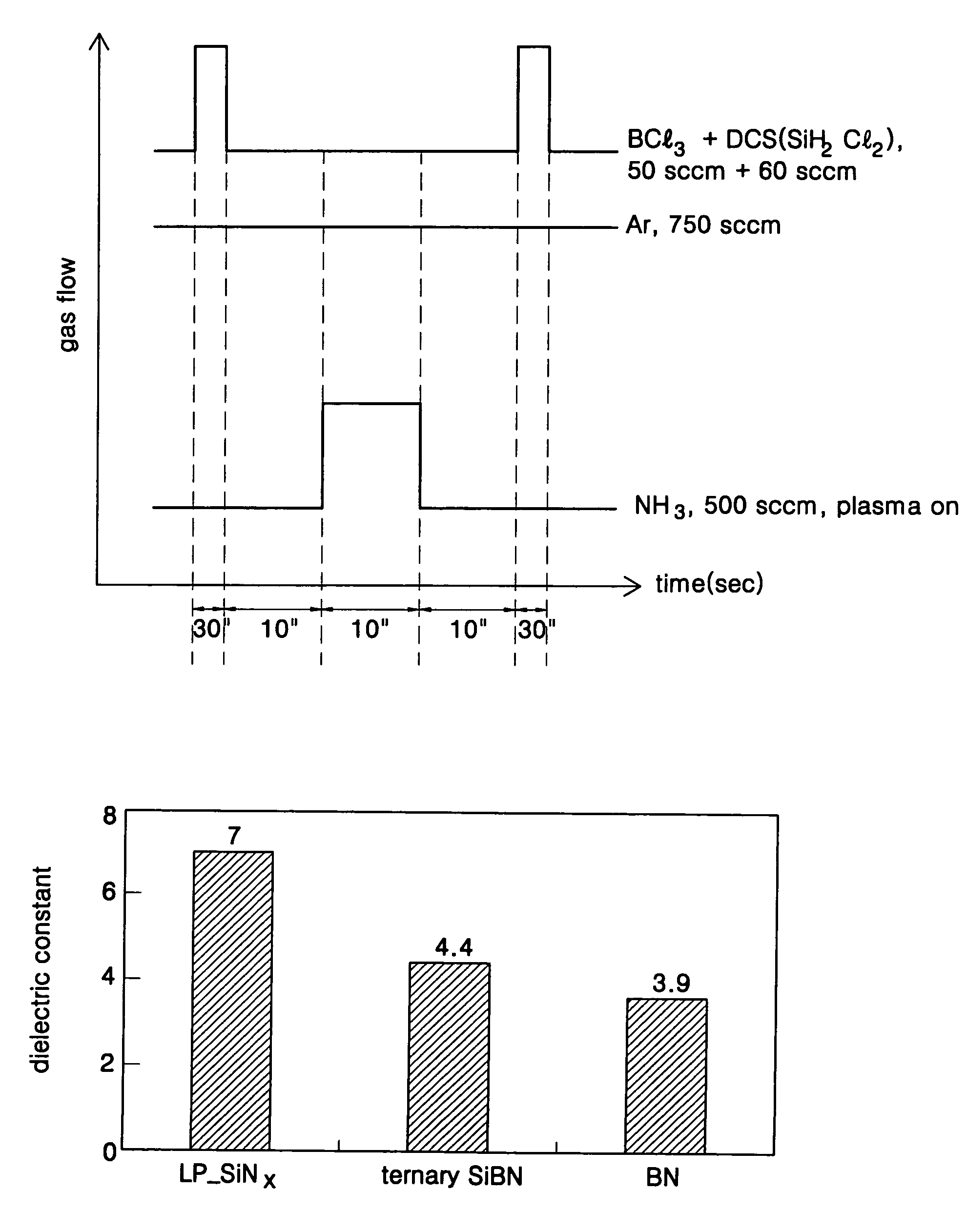
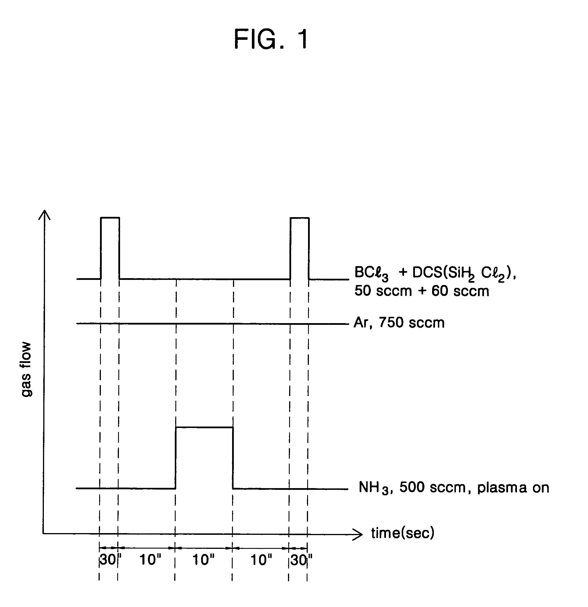
[0032]The present invention will now be described more fully hereinafter with reference to the accompanying drawings, in which exemplary embodiments of the invention are shown. The invention may, however, be embodied in different forms and should not be construed as limited to the embodiments set forth herein. Rather, these embodiments are provided so that this disclosure will be thorough and complete, and will fully convey the scope of the invention to those skilled in the art. In the figures, the dimensions of films, layers and regions are exaggerated for clarity of illustration. It will also be understood that when a layer is referred to as being “on” another layer or substrate, it can be directly on the other layer or substrate, or intervening layers may also be present. Further, it will be understood ...


PUM

PropertyMeasurementUnit
internal pressureaaaaaaaaaa
temperatureaaaaaaaaaa
dielectric constantaaaaaaaaaa

Abstract

A method for forming a low-k dielectric layer for a semiconductor device using an ALD process including (a) forming predetermined interconnection patterns on a semiconductor substrate, (b) supplying a first and a second reactive material to a chamber having the substrate therein, thereby adsorbing the first and second reactive materials on a surface of the substrate, (c) supplying a first gas to the chamber to purge the first and second reactive materials that remain unreacted, (d) supplying a third reactive material to the chamber, thereby causing a reaction between the first and second materials and the third reactive material to form a monolayer, (e) supplying a second gas to the chamber to purge the third reactive material that remains unreacted in the chamber and a byproduct; and (f) repeating (b) through (e) a predetermined number of times to form a SiBN ternary layer having a predetermined thickness on the substrate.

Description

[0001]This application is a continuation-in-part of application Ser. No. 10 / 378,681, filed Mar. 5, 2003 now U.S. Pat. No. 6,815,350.BACKGROUND OF THE INVENTION[0002]1. Field of the Invention[0003]The present invention relates to a method for forming a low-k dielectric layer for a semiconductor device. More particularly, the present invention relates to a method for forming a ternary silicon boron nitride (SiBN) layer having a low dielectric constant using an atomic layer deposition (ALD) process.[0004]2. Description of the Related Art[0005]Conventionally, a silicon nitride layer (SiNx) has been widely used in the manufacturing of semiconductor devices for several reasons. First, a SiNx layer has a high etching selectivity over a silicon oxide (SiO2) layer in a reactive ion etching (RIE) process and a wet etching process. Second, a SiNx layer exhibits strong oxidation and abrasion resistances. Third, a SiNx layer has an excellent diffusion barrier characteristic. However, a SiNx laye...

Claims


Application Information

Patent Timeline
Patent Type & Authority Patents(United States)
IPC IPC(8): C23C16/30H01L21/02H01L21/318C23C16/44H01L21/321C23C16/455
CPCC23C16/30C23C16/45531H01L21/318H01L21/3185H01L21/3211H01L21/02274H01L21/0228
Inventor AHN, JAE-YOUNGKIM, JIN-GYUNKIM, HEE-SEOKNO, JIN-TAEYANG, SANG-RYOLLEE, SUNG-HAEKIM, HONG-SUKLIM, JU-WANKIM, YOUNG-SEOKHYUNG, YONG-WOOKANG, MAN-SUG
Owner SAMSUNG ELECTRONICS CO LTD
Why Eureka
Try Eureka