Output circuit device for clock signal distribution in high-speed signal transmission

a clock signal and output circuit technology, applied in the field of signal transmission technology, can solve the problems of affecting the speed gap has been becoming a bottleneck in the performance of the computer, and the speed of signal transmission between the peripheral device and the processor/chipset is also becoming a major factor limiting the overall performance of the system, so as to minimize the occurrence of jitter, the effect of accurate timing and high speed

Inactive Publication Date: 2005-11-08
FUJITSU LTD
View PDF7 Cites 30 Cited by
  • Summary
  • Abstract
  • Description
  • Claims
  • Application Information

AI Technical Summary

Benefits of technology

[0010]An object of the present invention is to provide an output circuit device that can operate at high speed with accurate timing by minimizing the occurrence of jitter.

Problems solved by technology

Specifically, the speed gap between a memory such as a SRAM or DRAM and a processor (i.e., between LSIS), for example, has been widening, and in recent years, this speed gap has been becoming a bottleneck in a computer's performance.
Further, not only the speed of signal transmission between such chips, but because of increasing integration and increasing size of chips, decreasing supply voltage levels (decreasing signal amplitude levels), etc. the speed of signal transmission between elements or circuit blocks within a single chip is also becoming a major factor limiting the performance of the chip.
Moreover, the speed of signal transmission between a peripheral device and the processor / chipset also is becoming a major factor limiting the overall performance of the system.
In the prior art, it was difficult to provide an output circuit device that can operate at high speed with accurate timing by minimizing the occurrence of jitter.

Method used


Image

  • Output circuit device for clock signal distribution in high-speed signal transmission
  • Output circuit device for clock signal distribution in high-speed signal transmission
  • Output circuit device for clock signal distribution in high-speed signal transmission

Examples


first embodiment

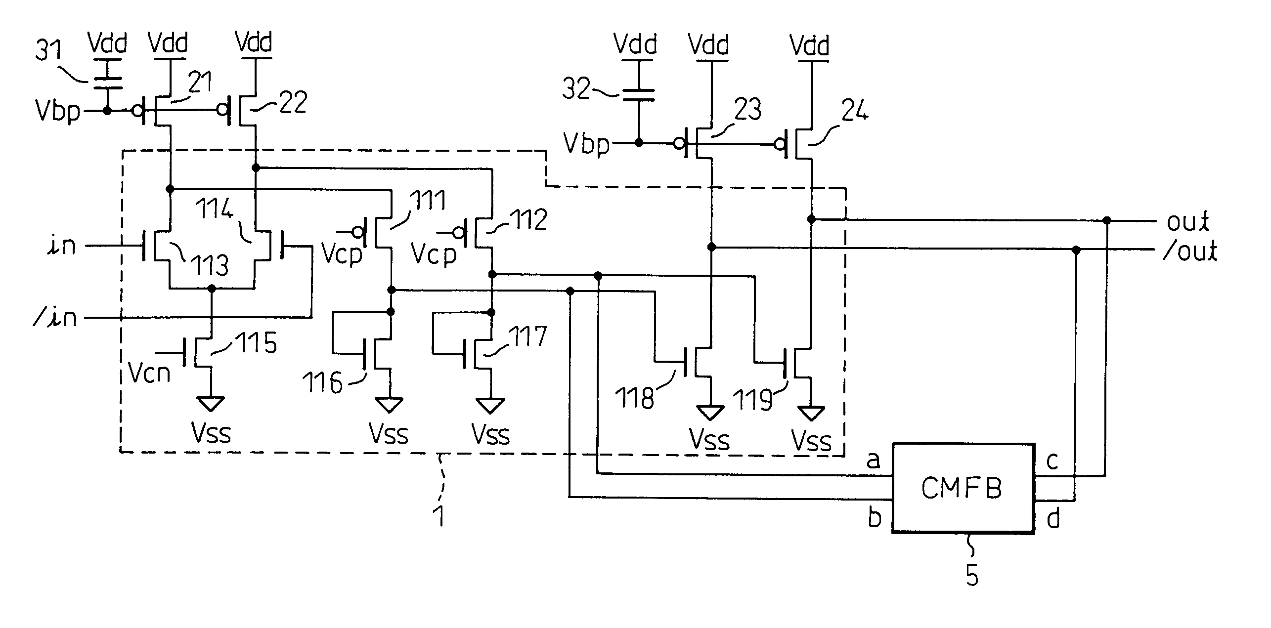
[0078]FIG. 6 is a block circuit diagram schematically showing the output circuit device according to the present invention. In FIG. 6, reference numeral 1 is a circuit proper (output circuit), 21 to 24 are isolating PMOS transistors, 31 and 32 are capacitors, and 5 is a common-mode feedback (CMFB) circuit.

[0079]In the circuit proper 1, input signals (input clocks) in and / in are received by an input amplifier circuit comprising an nMOS transistor differential pair 113, 114; the input signals are then transferred via pMOS transistors 111, 112 and nMOS transistors 116, 117, respectively, and output signals (output clocks) out and / out are produced via an output stage amplifier comprising nMOS transistors 118 and 119 respectively connected to the transistors 116 and 117 in a current-mirror configuration. Here, the transistors 111 and 112 are supplied at their gates with a constant voltage Vcp which is lower than the drain potential of the transistors 21 and 22 by a value not smaller than...

second embodiment

[0085]FIG. 8 is a circuit diagram schematically showing the output circuit device according to the present invention.

[0086]As shown in FIG. 8, in the output circuit device of the second embodiment, the differential input signals in and / in are supplied to the gates of transistors 121, 123 and transistors 122, 125, respectively, each transistor pair forming a push-pull circuit (inverter). The common source of the pMOS transistors 121 and 122 is connected to the high-level power supply line (Vdd) via an isolating pMOS transistor 20 and a low-pass filter circuit 6, and the gate of the transistor 20 is connected to the drain of a pMOS transistor 61 (the source of the transistor 20) via a capacitor 30. Here, the transistor 20 and the capacitor 30 correspond to the transistor 2a and the capacitor 3a, respectively, previously shown in FIG. 3A. In the second embodiment, however, the capacitor 30, one terminal of which is connected to the gate of the transistor 20, has its other terminal conn...

third embodiment

[0090]FIG. 9 is a circuit diagram schematically showing the output circuit device according to the present invention.

[0091]As is apparent from a comparison between FIG. 9 and FIG. 8, in the output circuit device of the third embodiment, a resistor (filter resistor) 63 is used in place of the pMOS transistor 61 in the low-pass filter circuit 6. Otherwise, the configuration is the same as that of the second embodiment shown in FIG. 8.


PUM


Abstract

An output circuit device has an output circuit connected between a first power supply line and a second power supply line via a control circuit having at least one isolating transistor. A control voltage held at a constant level is applied to a control electrode of the isolating transistor, and the control voltage is a voltage at a level that works to attenuate high-frequency components contained in a voltage supplied from the first or the second power supply line.

Description

CROSS REFERENCE TO RELATED APPLICATION[0001]This application is based upon and claims the benefit of priority from the prior Japanese Patent Application No. 2002-153885, filed on May 28, 2002, the entire contents of which are incorporated herein by reference. This application is a divisional of application Ser. No. 10 / 328,002, filed Dec. 26, 2002, now U.S. Pat. No. 6,812,777BACKGROUND OF THE INVENTION[0002]1. Field of the Invention[0003]The present invention relates to a signal transmission technology for enabling high-speed signal transmission between a plurality of LSI chips or a plurality of devices or circuit blocks within a single chip, or between a plurality of boards or cabinets, and more particularly to an output circuit device to be used for clock signal distribution in high-speed signal transmission, and a system constructed with such output circuit devices.[0004]2. Description of the Related Art[0005]Recently, the performance of components used in computers and other info...

Claims


Application Information

Patent Timeline
Patent Type & Authority Patents(United States)
IPC IPC(8): H03F3/45H03K5/00H03K19/0175
CPCH03F3/45192H03F3/45237H03F3/4565H03F3/45659H03F2203/45418H03F2203/45446
Inventor TAMURA, HIROTAKAKIBUNE, MASAYA
Owner FUJITSU LTD
Why Eureka
Try Eureka