Surface optical device apparatus, method of fabricating the same, and apparatus using the same

a surface optical device and apparatus technology, applied in the field of surface optical device apparatus, can solve the problems of poor thermal radiation characteristic, inferior luminary characteristics, light radiation efficiency and light output, and limitations on process freedom (i.e., plasma processing, processing temperature, etc.) to achieve the effect of improving productivity

Inactive Publication Date: 2005-11-29
CANON KK
View PDF27 Cites 40 Cited by
  • Summary
  • Abstract
  • Description
  • Claims
  • Application Information

AI Technical Summary

Benefits of technology

[0012]The present invention is generally directed to a surface optical device apparatus including a surface optical device, and a second substrate. The surface optical device includes a functional layer grown on a first substrate, which acts as a supporting substrate needed for fabricating the functional layer thereon, with the first substrate being later thinned or removed, and a first electrode formed on at least one of the surfaces of the functional layer. The surface optical device emits or receives light in a direction approximately perpendicular to the first substrate, and the first electrode has a function for electrically controlling the light emission or reception. The second substrate includes a second electrode formed thereon, and the surface optical device is bonded to the second substrate with the first electrode and the second electrode being in electrical contact with each other. In the apparatus of this invention, the first substrate is removed or thinned by etching or the like after the optical device is bonded to the second substrate, such as a Si substrate or a circuit substrate, with the first and second electrodes electrically connected, and another electrode is led from a surface of the optical device exposed after the first substrate is removed or thinned. Accordingly, the thermal characteristic of the surface optical device is improved due to the close proximity of the second substrate to an active layer of the optical device, and thus, no high alignment precision is required at the time of bonding the optical device. Further, the first substrate still remains after the optical device has been bonded, so that the optical device can be readily handled without damaging the functional layer.
[0075]According to this method, a plurality of the optoelectronic MCM's can be collectively fabricated by a single process, and productivity can be improved.

Problems solved by technology

There are significant problems with the structure disclosed in Japanese Patent Application Laid-Open No. 9(1997)-223848, however.
Its thermal radiation characteristic is poor, and its luminary characteristics, such as light radiation efficiency and light output, are inferior to those of ordinary implementation structures, since the polyimide layer 300 is interposed between the optical devices 100A and 100B and the Si substrate 200.
Further, since the fabrication process of the optical devices 100A and 100B is performed only after the functional layers of the optical devices are transferred to the Si substrate 200, limitations on the freedom of the process (i.e., on processing temperature, plasma processing, and the like) arise, due to concerns with preventing damage to the IC.
Accordingly, its handling is difficult, and its performance characteristics are likely to be decreased due to the introduction of crystallographic defects therein, and the like.
Therefore, high alignment precision is required, and costs increase accordingly.

Method used


Image

  • Surface optical device apparatus, method of fabricating the same, and apparatus using the same
  • Surface optical device apparatus, method of fabricating the same, and apparatus using the same
  • Surface optical device apparatus, method of fabricating the same, and apparatus using the same

Examples


first embodiment

[0092](First Embodiment)

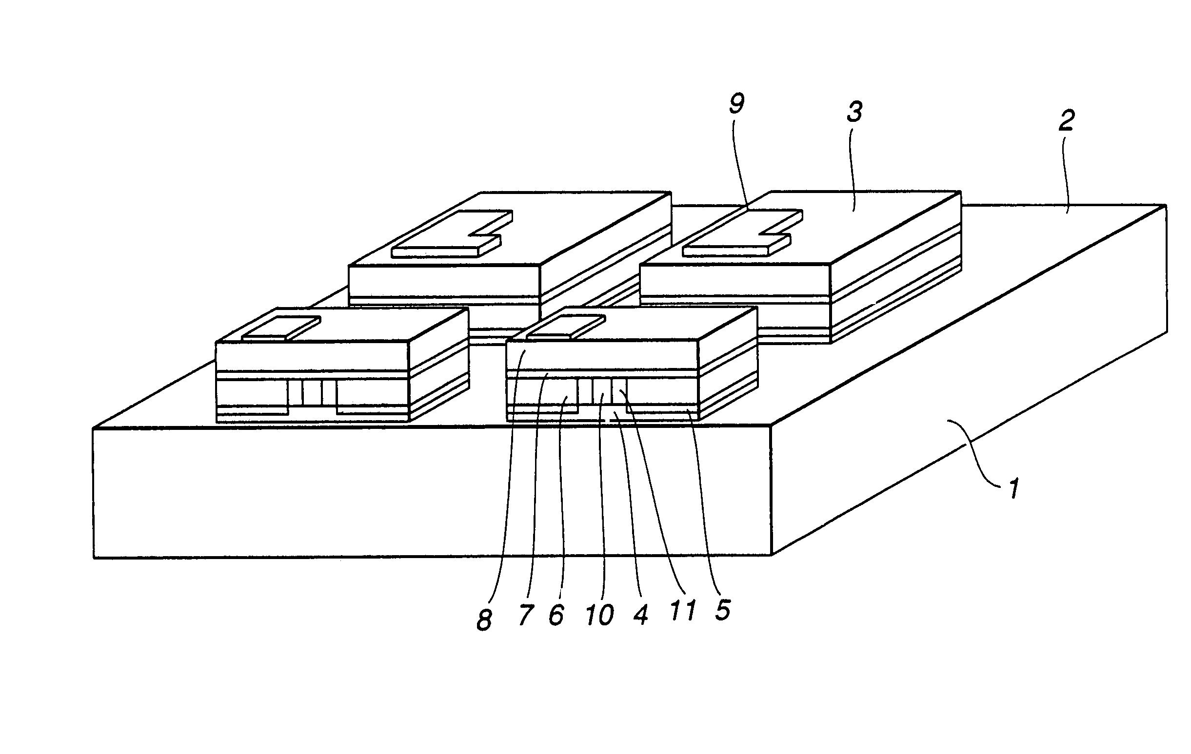
[0093]The first embodiment of the present invention is directed to a structure in which a surface emitting laser is used as the surface emitting device, and only its functional layer, including a light radiating layer and a mirror layer, is transferred to a ceramic substrate of AlN or the like having good thermal conductivity. FIG. 3 illustrates a perspective view of such a structure. In FIG. 3, the functional layer between the surface optical devices is completely removed.

[0094]An electrode 2 of Ti / Pt / Au is formed on an appropriate place of an AlN ceramic substrate 1 on which a surface emitting laser 3 is implemented, and this electrode 2 serves as a common electrode. A Ti / Pt / Au electrode 4 formed as a p-side electrode of the surface emitting laser 3 is thermally connected to the common electrode 2 with an Au / Sn solder (not shown) disposed on an appropriate portion of the electrode 2. Besides the solder formed by evaporation or plating, connection may be car...

second embodiment

[0116](Second Embodiment)

[0117]The second embodiment of the present invention is directed to a structure in which an electrode pattern is formed as a common electrode on an implementation substrate 1, and a thinned functional layer of a surface emitting laser 3 is simply aligned with and implemented on the implementation substrate 1. Where the number of devices 3 in an array increases, a wiring matrix as illustrated in FIG. 8 is advantageous in simplifying the structure of the electrical wiring. Therefore, the common electrode on the implementation substrate 1 is separated into a plurality of stripe-shaped portions.

[0118]The structure of the surface emitting laser 3 is similar to that of FIG. 3. An electrode pattern 60 of plural lines is formed on the AlN substrate 1 as illustrated in FIG. 8, and the functional layer of the surface emitting laser 3 is transferred onto the stripe-shaped electrode pattern 60 as in the first embodiment. The p-side electrodes of the devices 3 are separa...

third embodiment

[0123](Third Embodiment)

[0124]In the above embodiments, the process of fabricating an MCM is described. However, it is desirable that a collective process be carried out on a wafer to improve the productivity.

[0125]FIG. 10 illustrates this collective processing manner. In the third embodiment, a relatively inexpensive Si substrate is used. Regions 81, on which the device is implemented, are arranged in a two-dimensional array at predetermined intervals on the Si substrate 80. Electrodes are initially formed on the regions 81 on the wafer of the Si substrate 80 as in the first or second embodiment, a necessary number of arrays of surface emitting lasers 84 are cut out from a GaAs substrate 83, and the arrays of the surface emitting lasers 84 are implemented on the electrodes by a die-bonding apparatus, respectively. When the electrodes are formed by lithography, the electrodes can be arrayed with the precision of a photomask, and the device array 84 can be precisely implemented by th...


PUM

PropertyMeasurementUnit
thicknessaaaaaaaaaa
diameteraaaaaaaaaa
sizeaaaaaaaaaa

Abstract

A surface optical device apparatus includes a surface optical device and a second substrate. The surface optical device includes a functional layer grown on a first substrate, which acts as a supporting substrate for fabricating the functional layer thereon. The first substrate is later thinned or removed, and a first electrode is formed on at least one of surfaces of the functional layer. The surface optical device performs light emission or light reception along a direction approximately perpendicular to the first substrate, and the first electrode has functionality for electrically controlling the light emission or reception. The second substrate includes a second electrode formed thereon, and the surface optical device is bonded to the second substrate with the first electrode and the second electrode in electrical contact with each other.

Description

[0001]This application is a division of U.S. application Ser. No. 10 / 429,805, filed May 6, 2003; now U.S. Pat. No. 6,836,579, which is a continuation of U.S. application Ser. No. 09 / 645,317, filed Aug. 25, 2000, now abandoned.BACKGROUND OF THE INVENTION[0002]1. Field of the Invention[0003]This invention relates to a surface optical device apparatus which can be readily fabricated with good yield and is suitable for use in a structure constructed in a one- or two-dimensional array, its fabrication method, an optoelectronic device in which the surface optical device is integrated together with a Si integrated circuit (Si-IC), an optical wiring device using the surface optical device apparatus, an optical recording apparatus using the surface optical device apparatus, and related structures and devices.[0004]2. Related Background Art[0005]In recent years, the development of surface light emitting devices arranged in two-dimensional arrays has been desired. Among such devices, a vertica...

Claims


Application Information

Patent Timeline
Patent Type & Authority Patents(United States)
IPC IPC(8): H01S5/42B41J2/45G01D9/42G02B6/12G02B6/26G02B6/42G11B7/12G11B7/22G11B11/105H01S5/02H01S5/022H01S5/042H01S5/40
CPCB41J2/45G11B7/1205G11B7/22G11B11/10532H01L2221/6835H01L2221/68354H01L2221/68363H01L2221/68368H01S5/0217H01S5/02248H01S5/02272H01S5/0425H01S5/18311H01S5/423G11B7/123H01S5/0216H01S5/18305H01S5/04256H01S5/02325H01S5/02345H01S5/0237
Inventor OUCHI, TOSHIHIKO
Owner CANON KK
Why Eureka
Try Eureka