Use of atomic oxygen process for improved barrier layer

a technology of atomic oxygen and barrier layer, which is applied in the direction of semiconductor devices, semiconductor/solid-state device details, electrical apparatus, etc., can solve the problems of affecting the reliability and performance of fabricated integrated circuits, the reliability of electrical contacts is increasingly defining the limits of performance and density of modern very-large-scale integrated circuits

Inactive Publication Date: 2005-12-06
MICRON TECH INC
View PDF30 Cites 12 Cited by
  • Summary
  • Abstract
  • Description
  • Claims
  • Application Information

AI Technical Summary

Benefits of technology

[0009]The present invention provides a composite barrier layer formed between a glass insulating layer and active regions of a memory device, for example a DRAM device, to eliminate the diffusion of impurity atoms from the glass insulating layer into the active regions of the device.

Problems solved by technology

The integration of a large number of components on a single IC chip requires complex interconnects.
Because of their increasing importance, the qualities of the interconnect structures drastically affect the reliability and performance of fabricated integrated circuits.
Currently, the reliability of electrical contacts are increasingly defining the limits in performance and density of modern very-large scale integrated (VLSI) circuits.
A major drawback posed by the migration of impurity boron / phosphorous atoms at the source / drain-BPSG interface 51 is the decrease in the “refresh time” of the DRAM device, and consequently an increase in the DRAM error rate.
While the composite barrier layer 52 suppresses the diffusion of the boron / phosphorous impurity atoms at the source / drain-BPSG interface 51, there is a problem in that the deposition of the TEOS liner 52a is highly non-conformal.

Method used


Image

  • Use of atomic oxygen process for improved barrier layer
  • Use of atomic oxygen process for improved barrier layer
  • Use of atomic oxygen process for improved barrier layer

Examples


Embodiment Construction

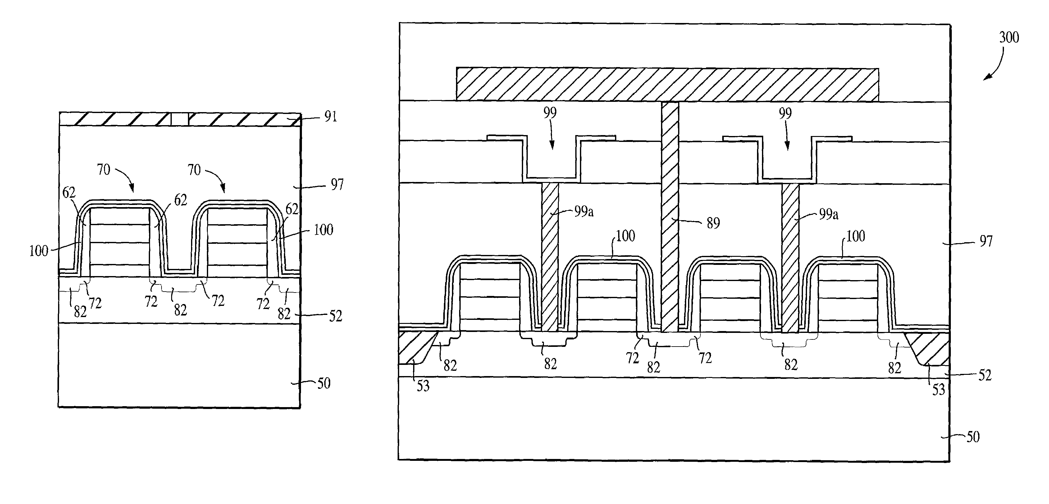
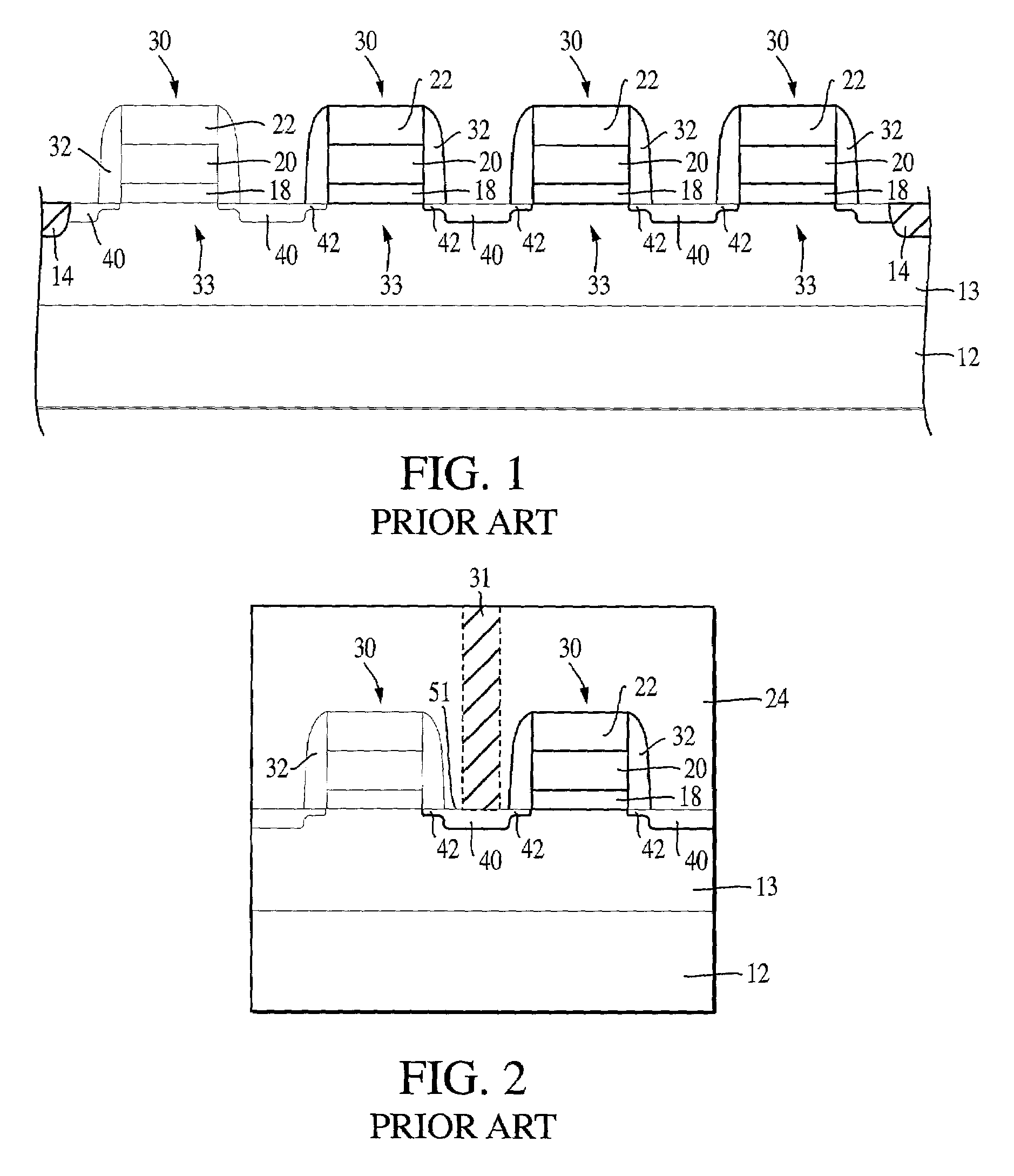
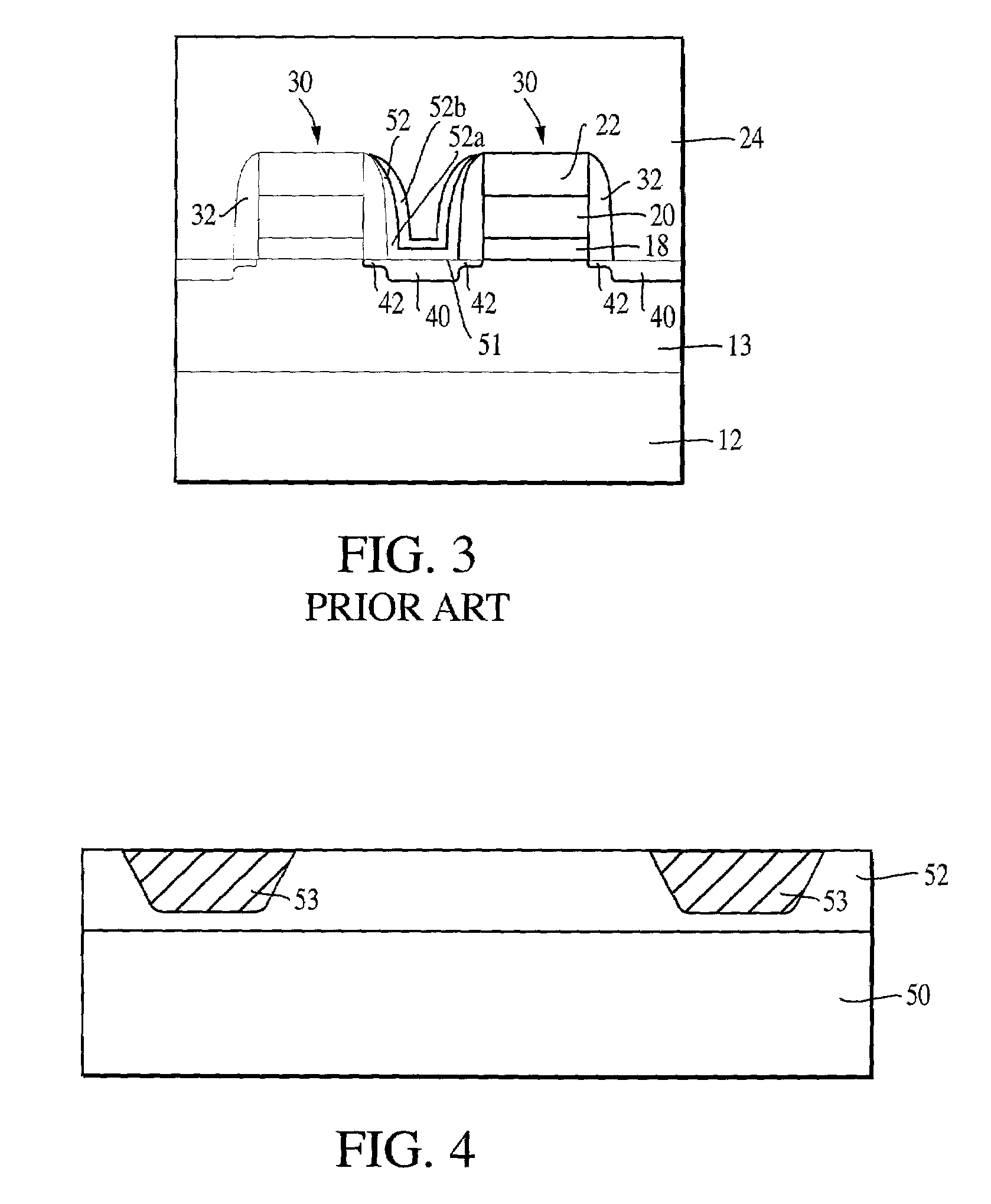
[0033]In the following detailed description, reference is made to various specific exemplary embodiments in which the invention may be practiced. These embodiments are described with sufficient detail to enable those skilled in the art to practice the invention, and it is to be understood that other embodiments may be employed, and that structural, logical, and electrical changes may be made.

[0034]The terms “wafer” or “substrate” used in the following description may include any semiconductor-based structure that has a semiconductor surface. Wafer and structure must be understood to include silicon-on insulator (SOI), silicon-on sapphire (SOS), doped and undoped semiconductors, epitaxial layers of silicon supported by a base semiconductor foundation, and other semiconductor structures. The semiconductor need not be silicon-based. The semiconductor could be silicon-germanium, germanium, or gallium arsenide.

[0035]Referring now to the drawings, where like elements are designated by lik...


PUM

PropertyMeasurementUnit
temperatureaaaaaaaaaa
thicknessaaaaaaaaaa
temperatureaaaaaaaaaa

Abstract

A composite barrier layer formed between a glass film and active regions of a memory device is disclosed. The composite barrier layer comprises an oxide layer formed by atomic deposition process and an insulating layer, for example a nitride barrier layer, formed over the oxide layer. The composite barrier layer eliminates the diffusion of impurity atoms from the glass film into the active regions of the device.

Description

FIELD OF THE INVENTION[0001]The present invention relates to the field of semiconductor devices and, in particular, to a method of increasing the performance of such devices.BACKGROUND OF THE INVENTION[0002]The integration of a large number of components on a single IC chip requires complex interconnects. Ideally, the interconnect structures should be fabricated with minimal signal delay and optimal packing density. Because of their increasing importance, the qualities of the interconnect structures drastically affect the reliability and performance of fabricated integrated circuits. Currently, the reliability of electrical contacts are increasingly defining the limits in performance and density of modern very-large scale integrated (VLSI) circuits.[0003]A conventional pair of transistors for integrated memory cells is illustrated in FIG. 1. Respective access transistors 33 are formed within a well 13 of a semiconductor substrate 12. The well and transistors are surrounded by a fiel...

Claims


Application Information

Patent Timeline
Patent Type & Authority Patents(United States)
IPC IPC(8): H01L21/314H01L21/768H01L21/8234H01L21/8242H01L23/31H01L27/108
CPCH01L21/76828H01L21/76832H01L21/76834H01L21/823425H01L21/823475H01L23/3192H01L27/10873H01L21/3145H01L27/10811H01L27/10855H01L27/10888H01L2924/19041H01L2924/0002H01L2924/00H10B12/312H10B12/0335H10B12/05H10B12/485
Inventor WEIMER, RONALD A.PING, ER-XUAN
Owner MICRON TECH INC
Why Eureka
Try Eureka