Enhanced T-gate structure for modulation doped field effect transistors

a field effect transistor and modulation doped technology, applied in the field of modulation doped field effect transistors, can solve the problems of increasing gate resistance, increasing the complexity of technology, and needing new methods, so as to reduce parasitic capacitance, improve yield, and high scalable

Inactive Publication Date: 2005-12-06
GLOBALFOUNDRIES US INC
View PDF9 Cites 18 Cited by
  • Summary
  • Abstract
  • Description
  • Claims
  • Application Information

AI Technical Summary

Benefits of technology

[0017]In accordance with the objects listed above, the present invention describes an enhanced T-gate structure that has a thin insulating layer with a low dielectric constant disposed on the neck of the T-gate. This insulating layer provides additional mechanical support and protects the vulnerable neck of the T-gate from chemical attack during subsequent device processing, making the T-gate structure highly scalable and improving yield. By using a thin conformal insulating layer with a low dielectric constant it is possible to reduce the parasitic capacitances associated with the fringing fields surrounding the gate. This insulating layer can also make it possible to reduce the source-to-gate spacing because metal can be deposited in a self-aligned manner under the overhang of the T-gate without shorting the source and gate, in contrast to the prior art supported T-gate of FIG. 2.

Problems solved by technology

As devices are scaled down, however, the technology becomes more complex and new methods are needed to maintain the expected performance enhancement from one generation of devices to the next.
State-of-the-art MODFETs typically increase device speed (often characterized in terms of the unity gain frequency ft) by shrinking the gate length to reduce carrier transit times. However, shrinking the gate dimensions also increases the gate resistance, RG, adversely affecting several aspects of device performance.
However, the top-heavy geometry of the free T-gate gives these structures an inherent mechanical instability, resulting in poor yield.
In addition, the neck portion of the T-gate is also extremely vulnerable to chemical attack during subsequent processing.
These yield issues, aggravated by shrinking gate lengths, impose severe limitations on the ultimate scalability and applicability of free T-gate structures for MODFET circuits.
The yield problem associated with T-gates is highlighted by the fact that even though individual SiGe MODFET devices with excellent characteristics have been fabricated, there have been few demonstrations of circuits fabricated using these devices.
Dielectric supports with the prior art geometry of FIG. 2C completely fill the volume under the T-bar portion overhang, a potential disadvantage if additional conductive layers are to be deposited, since conductive material may unintentionally accumulate on the exposed edges of the supports and short the source / drain regions (not shown) to the gate.
T-gates thus formed have a relatively high-k dielectric completely underfilling the overhang of the free T-gate that results in a considerable increase in the parasitic gate capacitance associated with the fringing fields present in the dielectric surrounding the gate.
However, the source-to-gate spacing is still limited by the width of the overhang of the T-bar portion of the T-gate.

Method used


Image

  • Enhanced T-gate structure for modulation doped field effect transistors
  • Enhanced T-gate structure for modulation doped field effect transistors
  • Enhanced T-gate structure for modulation doped field effect transistors

Examples


Embodiment Construction

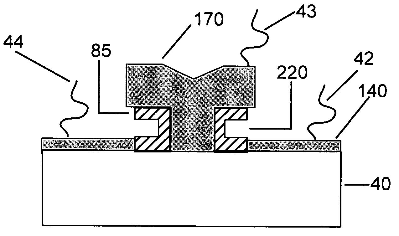
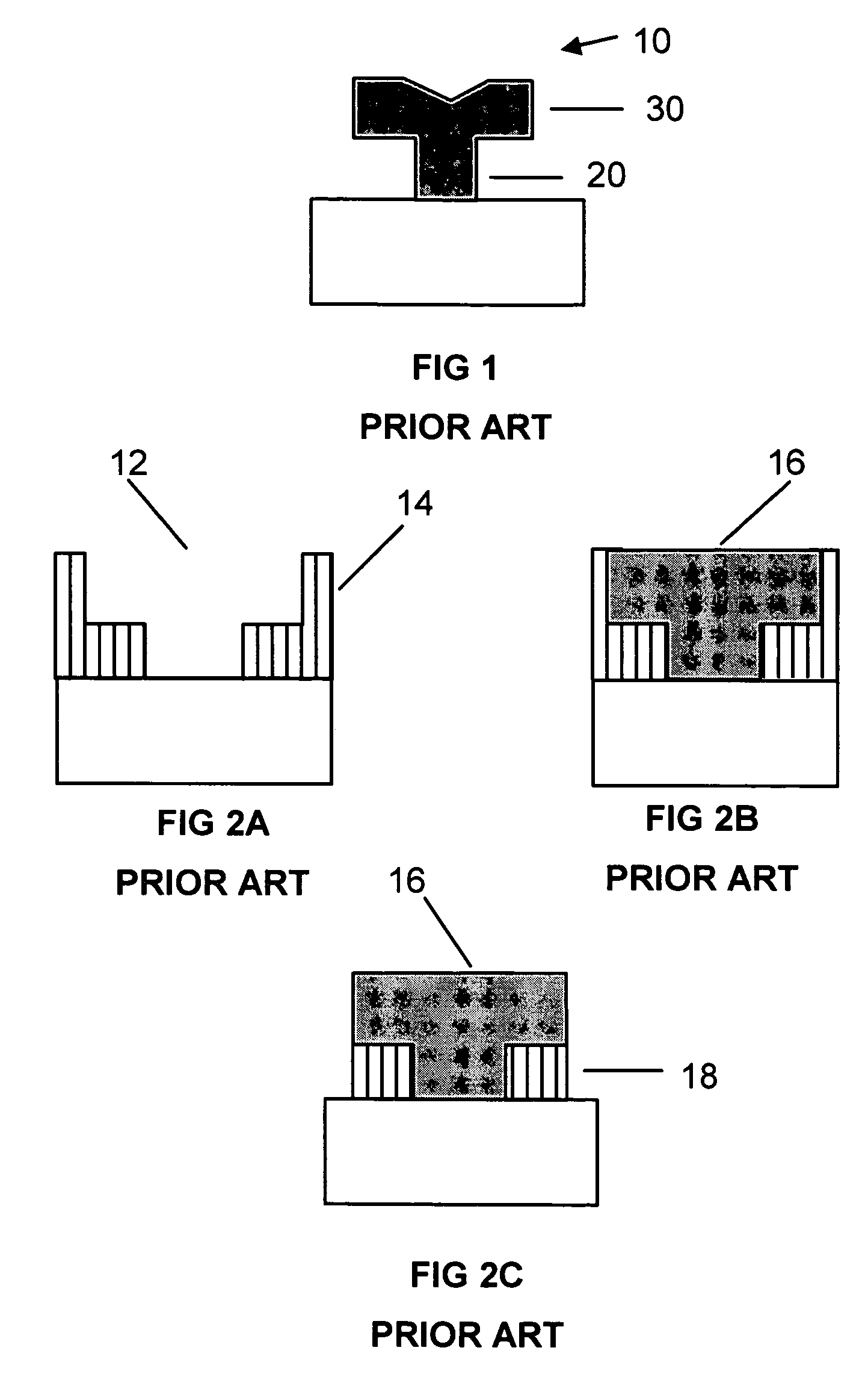
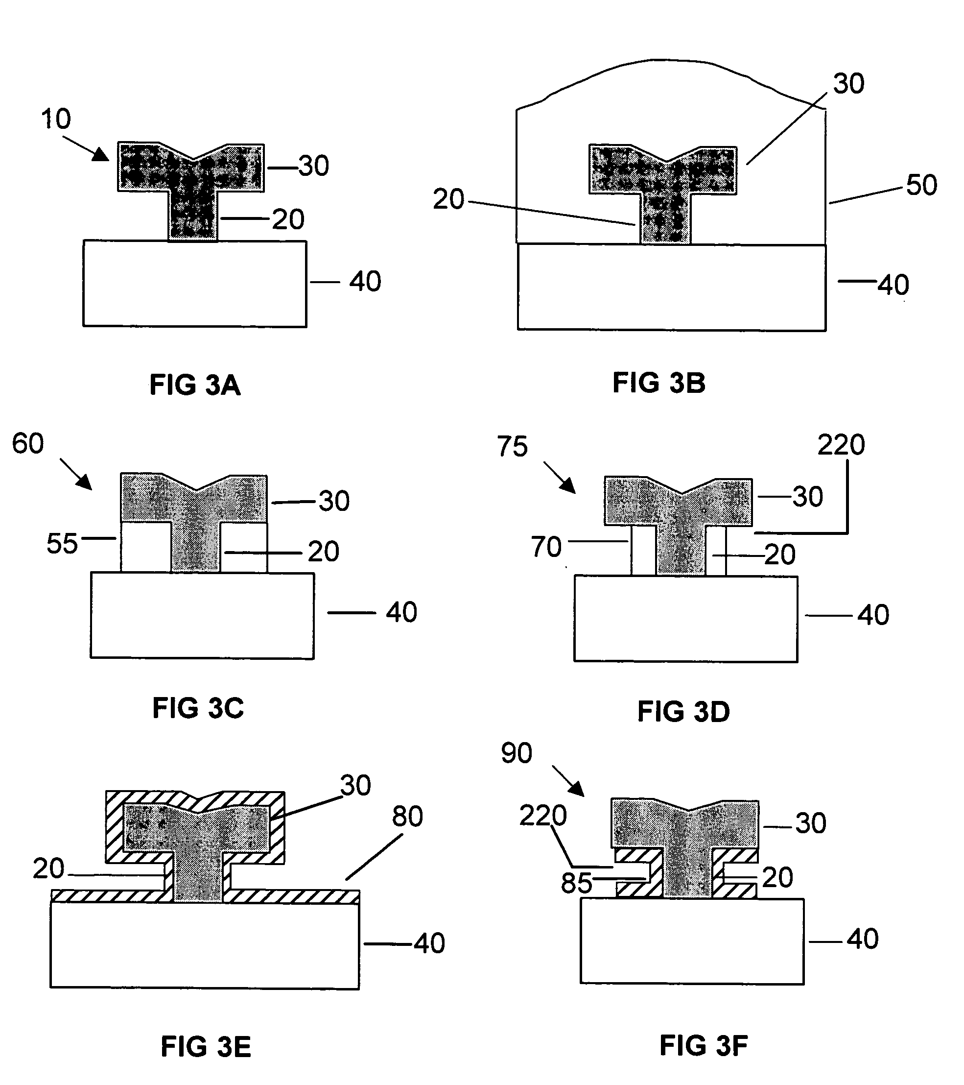
[0029]FIG. 1 shows prior art in a cross-sectional view of a free (freestanding) T-gate 10 formed by conventional processing. T-gates are typically formed using a stack of metals, e.g. Ti / Pt / Au for state-of-the-art Si / SiGe p-MODFETS, where Ti is used for the gate contact because of its high Schottky barrier on p-type Si. Alternate gate stacks may be used depending on the gate work function desired. For example, the T-bar and neck portions of the T-gate may be formed from any conductive material, including metals (for example Al, Au, Co, Ir, Mo, Nb, Ni, Pd, Pt, re, Ru, Ti, Ta, and W), conductive nitrides and silicides; layers of these materials, combinations of these materials. The T-gate has a neck portion 20, which rests on the surface that the whole T-gate is standing on. The neck portion is topped by the T-bar portion 30. The T-bar portion has overhangs which extend beyond the neck portion by a certain width. There is an empty volume under the overhang, bounded on three sides by t...


PUM


Abstract

A structure and a method are disclosed of an enhanced T-gate for modulation doped field effect transistors (MODFETs). The enhanced T-gate has insulator spacer layers sandwiching the neck portion of the T-gate. The spacer layers are thinner than the T-bar portion overhang. The insulating layer provides mechanical support and protects the vulnerable neck portion of the T-gate from chemical attack during subsequent device processing, making the T-gate structure highly scalable and improving yield. The use of thin conformal low dielectric constant insulating layers ensures a low parasitic gate capacitance, and reduces the risk of shorting gate and source metallurgy when source-to-gate spacings are reduced to smaller dimensions.

Description

[0001]This application is a division of application Ser. No. 10 / 207,352, filed Jul. 29, 2002, now U.S. Pat. No. 6,740,535.GOVERNMENT SUPPORT[0002]This invention was made with Government support under contract: N66001-99-C-6000, awarded by the Department of the Navy. The Government has certain rights in this invention.FIELD OF THE INVENTION[0003]The present invention relates to semiconductor devices and more specifically to modulation doped field effect transistors (MODFETs) having a conductive T-shaped gate. A structure and method are disclosed which allow for higher device performance and better T-gate scalability.BACKGROUND OF THE INVENTION[0004]Today's integrated circuits include a vast number of transistor devices formed in a variety of semiconductor materials. Smaller devices are the key to enhanced performance and to increased reliability. As devices are scaled down, however, the technology becomes more complex and new methods are needed to maintain the expected performance en...

Claims


Application Information

Patent Timeline
Patent Type & Authority Patents(United States)
IPC IPC(8): H01L21/285H01L29/423
CPCH01L29/42316H01L21/28587
Inventor SINGH, DINKARSAENGER, KATHERINE LYNNPATEL, VISHNUBHAI V.GRILL, ALFREDKOESTER, STEVEN JOHN
Owner GLOBALFOUNDRIES US INC
Why Eureka
Try Eureka