Laser diode array, laser device, wave-coupling laser source, and exposure device

a laser array and laser technology, applied in semiconductor lasers, instruments, optical elements, etc., can solve the problems of increasing manufacturing cost and maintenance cost, poor wavelength-conversion efficiency, and difficult to obtain high output power of wavelength conversion lasers in which infrared light is converted to its third harmonic, etc., to achieve fine image, sufficient focal depth, and sharp image

Inactive Publication Date: 2005-12-13
ADTEC ENG +1
View PDF20 Cites 41 Cited by
  • Summary
  • Abstract
  • Description
  • Claims
  • Application Information

AI Technical Summary

Benefits of technology

[0069]Further, in the fields of printing and medical images or in the case where an image formed by a print circuit board, a plasma display, liquid crystal display or the like is recorded on a photosensitive material by exposure, a fine image can be obtained when the multimode optical fiber is not larger than 50 μm in core diameter. Further, when the multimode optical fiber is not larger than 0.3 in numerical aperture NA, a sufficient focal depth can be ensured and a sharp image can be obtained.
[0070]When the wave-coupling laser source of the present inven

Problems solved by technology

In order to use as the exposure light source, the excimer laser is too large in size, which increases the manufacturing cost and the maintenance cost.
The wavelength conversion laser in which infrared light is converted to its third harmonic is very difficult to obtain high output power due to its very poor wavelength-conversion efficiency.
Further, use of an expensive wavelength conversion element adds to the cost of such a wavelength conversion laser.
Further, use of the Ar-laser encounters a difficulty that the Ar-laser

Method used


Image

  • Laser diode array, laser device, wave-coupling laser source, and exposure device
  • Laser diode array, laser device, wave-coupling laser source, and exposure device
  • Laser diode array, laser device, wave-coupling laser source, and exposure device

Examples


second embodiment

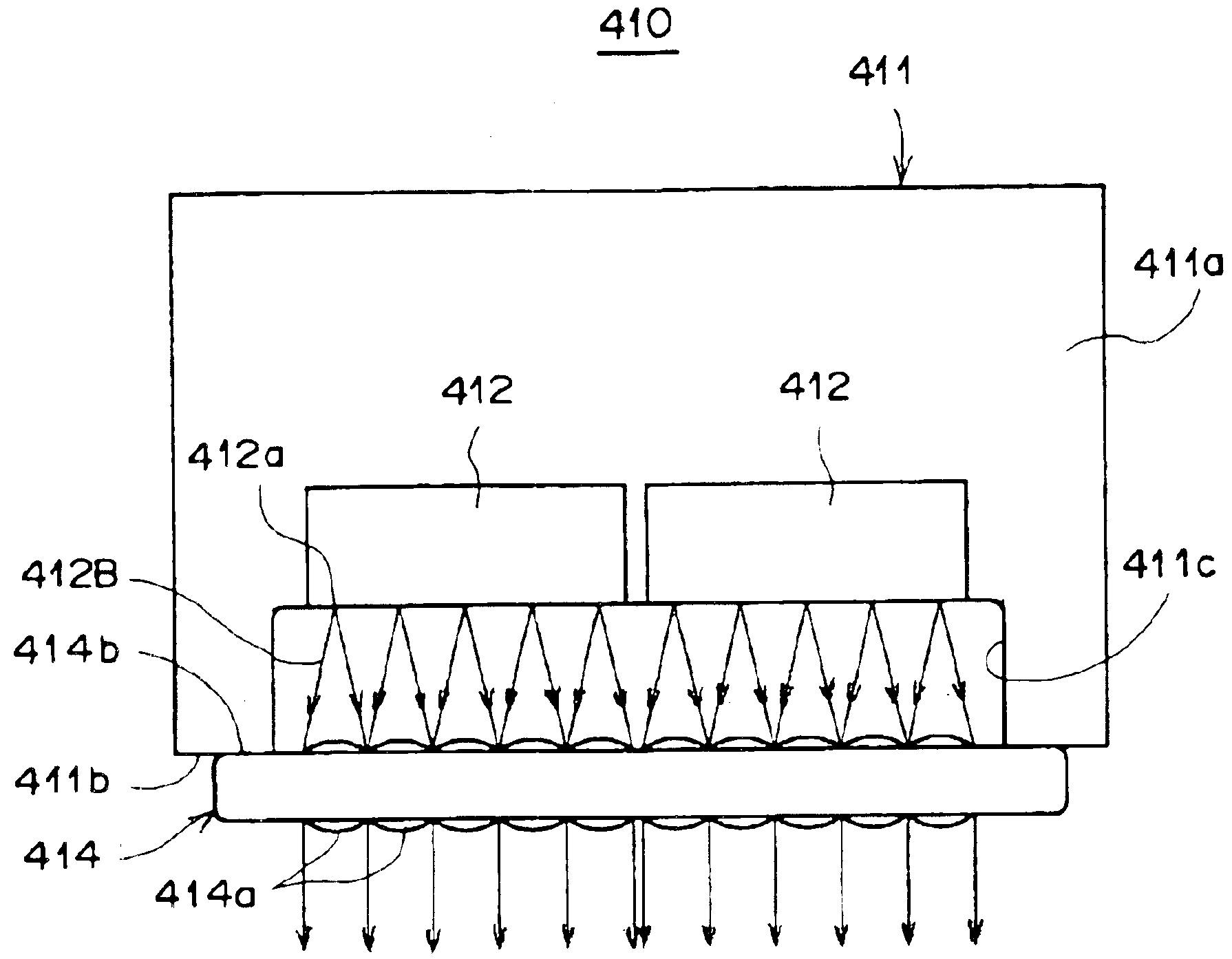
[0163]The laser device 410′ of this embodiment basically differs from that of the second embodiment shown in FIGS. 11 to 13 in that four multi-cavity laser diode chips 412 are arranged in two rows and two columns. That is, a second heat block 411′ the same as the heat block 411 described above is placed on the heat block 411 and fixed to the same. A pair of multi-cavity laser diode chips 412 and a collimator lens array 414 are fixed to each of the heat blocks 411 and 411′. The second heat block 411′ is substantially of the same structure as the heat block 411 and is provided with a recess 411c for preventing eclipse of the laser beams 412B. The second heat block 411′ is further provided with a recess 411d for preventing interference with the multi-cavity laser diode chips 412 fixed to the lower heat block 411.

[0164]Also in this embodiment, by moving the collimator lens array 414 up and down and left and right in a plane perpendicular to the optical axes of the lens elements 414a whi...

fifth embodiment

[0173]A wave-coupling laser source in accordance with the present invention will be described, hereinbelow. As shown in FIG. 18, the wave-coupling laser source of this embodiment comprises seven transverse multimode GaN-laser diode chips LD1, LD2, LD3, LD4, LD5, LD6 and LD7 fixed on a heat block 10 of Cu, seven collimator lens arrays 11 to 17 each for one of the seven laser diode chips LD1 to LD7, a condenser lens 20 and a multimode optical fiber 30. Each of the GaN-laser diode chips is a multi-cavity laser diode chip having a plurality of (three in this particular embodiment) light emitting points.

[0174]FIG. 18 shows the basic structure of a wave-coupling laser source in accordance with the fifth embodiment of the present invention, and the collimator lens arrays 11 to 17 and the condenser lens 20 are shown only schematically. Especially, though not clearly shown in FIG. 18, each of the collimator lens arrays 11 to 17 comprises a plurality of collimator lens elements which are the ...

sixth embodiment

[0185]A wave-coupling laser source in accordance with the present invention will be described with reference to FIG. 23, hereinbelow. In FIG. 23, elements analogous to those shown in FIG. 18 are given the same reference numerals and will not be described here unless necessary.

[0186]The wave-coupling laser source of this embodiment basically differs from that of the fifth embodiment in that a single collimator lens array 50 where collimator lens elements 50a for all the cavities of the laser diode chips LD1 to LD7 are integrated is employed in place of 7 collimator lens arrays 11 to 17.

[0187]Though the efficiency of utilization of space can be improved by closely arranging the 7 collimator lens arrays 11 to 17 of the structure described above and closely arranging the laser diode chips LD1 to LD7, the efficiency of utilization of space can be further improved by the use of the single collimator lens array 50. At the same time, when the efficiency of utilization of space is improved, ...


PUM


Abstract

A plurality of multi-cavity laser diode chips, each having a plurality of light emitting points, are fixed side by side and form a laser diode array.

Description

BACKGROUND OF THE INVENTION[0001]1. Field of the Invention[0002]This invention relates to a laser diode array, and more particularly to a laser diode array comprising a plurality of multi-cavity laser diode chips, each having a plurality of light emitting points, fixed side by side.[0003]This invention further relates to a laser device, a wave-coupling laser source and an exposure device using such a laser diode array.[0004]2. Description of the Related Art[0005]As devices for generating a laser beam in an ultraviolet region, there have been put into practice, for instance, a wavelength conversion laser in which infrared light generated from a semiconductor-laser-pumped solid state laser is converted to its third harmonic in an ultraviolet region, an excimer laser, and an Ar-laser.[0006]Further, GaN-semiconductor lasers radiating a laser beam substantially at 400 nm have been recently provided as shown in “Jpn. Appl. phys. Lett.”, Vol. 37, p. L1020.[0007]A light source radiating a l...

Claims


Application Information

Patent Timeline
IPC IPC(8): H01S5/022H01S5/02G02B6/42H01S5/323H01S5/40H01S5/10G02B27/09H01S5/023H01S5/0233
CPCG02B27/09H01S5/4031H01S5/32341H01S5/02216H01S5/02284H01S5/02236H01S5/02252H01S5/0224G02B6/4206H01S5/02469H01S5/4043H01L2224/48091H01S5/02326H01S5/0234H01S5/023H01S5/0233H01S5/0235H01S5/02251H01L2924/00014
Inventor NAGANO, KAZUHIKOOKAZAKI, YOJIKURAMACHI, TERUHIKO
Owner ADTEC ENG
Why Eureka
Try Eureka