This helps you quickly interpret patents by identifying the three key elements:
Problems solved by technology
Method used
Benefits of technology
Benefits of technology
[0022]The present invention was devised in view of the foregoing problem, and its object is to provide a semiconductor device which prevents a function element (circuit element, semiconductor element) such as a memory element and a logic element formed in each of plural semiconductor chips stacked on a stacking base from being damaged in terms of an electric property, and prevents the wire bonding strength from dropping, and allows a fine wiring pitch of wirings for relaying a wire-bonding wire to be formed thereon.
[0024]According to the arrangement, the interposer chip having one or more connection wirings is provided, for example, between the stacked semiconductor chips, or on the stacking base so as to be positioned on the upper side in a stacking direction. Further, the externally leading electrode provided on the semiconductor chip is connected to the connection wiring of the interposer chip, and relays the connection wiring so as to be electrically connected to an electrode of the stacking base or another semiconductor chip. In this manner, when connecting the externally leading electrode provided on the semiconductor chip to the electrode of the stacking base or another semiconductor chip, it is possible to relay the interposer chip, so that it is possible to shorten the length of a wire in wire bonding. Thus, it is possible to suppress such a problem that: the wire becomes brittle when the wire is long, and the wire hangs down due to its weight, which causes the wire to touch another wire and causes the wire to touch an edge of the lower semiconductor chip.
[0026]Further, in the conventional semiconductor device in which the rewiring layer is provided on the semiconductor chip, the rewiring layer is formed after forming a bonding pad on the semiconductor chip as an electrode. Thus, it is necessary to form and remove an etchingresist, so that an impure material remains on a surface of the bonding pad. As a result, the connection strength in wire bonding drops. On the other hand, in the structure according to the present invention, the rewiring layer is not formed, so that the connection strength in wire bonding does not drop. Further, in the conventional semiconductor device, when a stress is exerted on the rewiring layer in wire bonding, the wirings of the semiconductor chip positioned beneath the rewiring layer may be damaged. However, in the structure according to the present invention, a thickness and hardness of the interposer chip prevent the stress exerted in wire bonding.
[0027]Thus, according to the arrangement, it is possible to prevent the semiconductor element formed in each of the plural semiconductor chips stacked on the stacking base from deteriorating in terms of an electric property and from being physically damaged, and it is possible to improve the wire bonding strength.
Problems solved by technology
Thus, it is possible to suppress such a problem that: the wire becomes brittle when the wire is long, and the wire hangs down due to its weight, which causes the wire to touch another wire and causes the wire to touch an edge of the lower semiconductor chip.
Method used
Image
Click on the blue label to locate the original text in one second.
Reading with bidirectional positioning of images and text.
Examples
embodiment 1
[Embodiment 1]
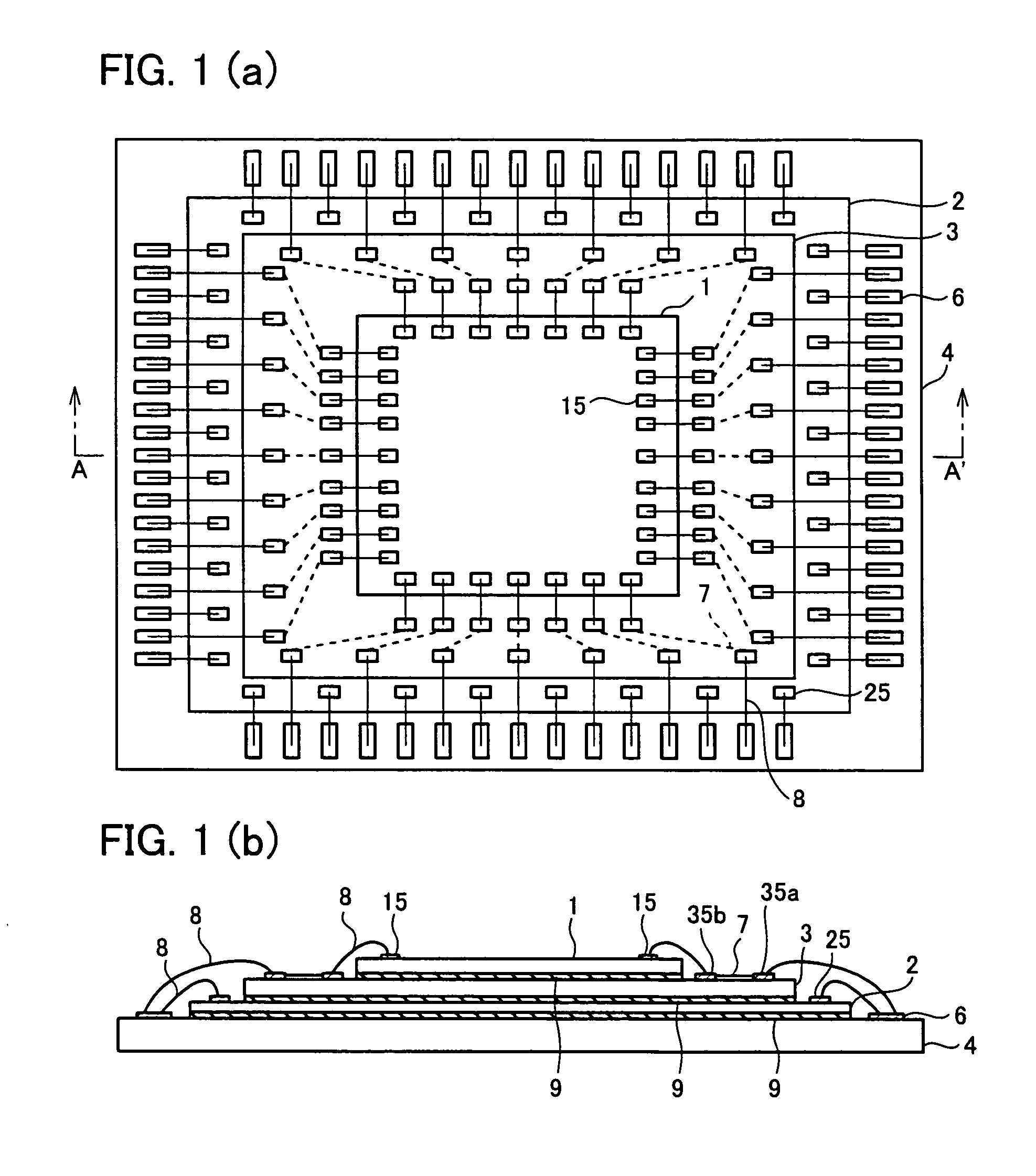
[0043]The following description will explain one embodiment of the semiconductor device of the present invention with reference to FIG. 1(a) and FIG. 1(b). Note that, the present invention is not limited to this.
[0044]FIG. 1(a) is a plan view obtained by viewing the semiconductor device of the present embodiment from above in a stacking direction, and FIG. 1(b) is a cross sectional view taken along A–A′ of FIG. 1(a).
[0046]As shown in FIG. 1 (a) and FIG. 1 (b), the semiconductor device of the present embodiment is arranged so that: a substrate 4 is used as a stacking base, and a semiconductor chip 2, an interposer chip 3, and a semiconductor chip 1 are stacked on and above the stacking base in this order. Note that, by using die-bonding layers 9, the substrate 4 and the semiconductor chip 2 are bonded to each other, and the semiconductor chip 2 and the interposer chip 3 are bonded to each other, and the interposer chip 3 and ...
embodiment 2
[Embodiment 2]
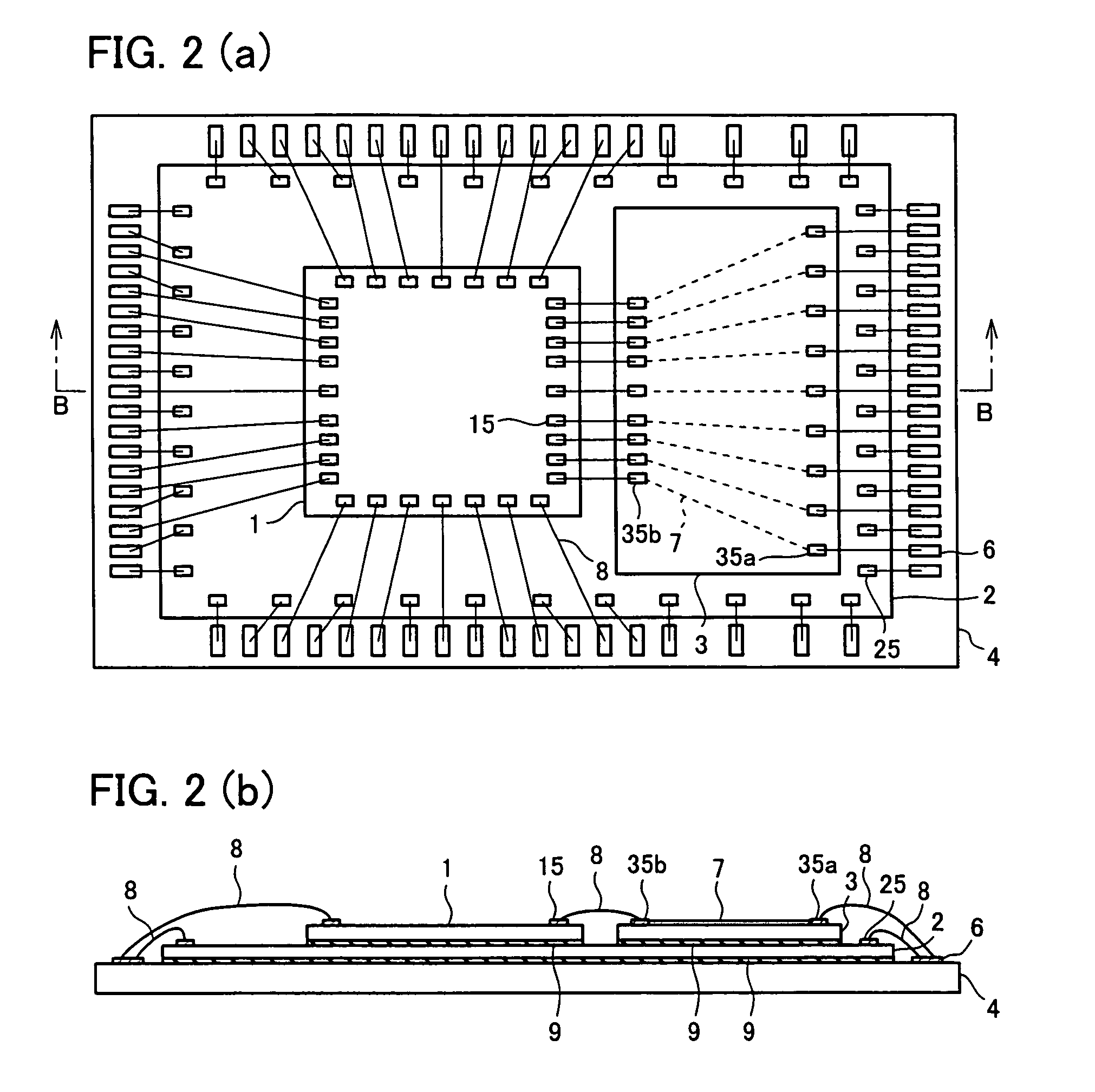
[0064]The following description will explain another embodiment of the semiconductor device of the present invention with reference to FIG. 2(a) and FIG. 2(b). Note that, for convenience in description, same reference signs are given to members having the same function as members described in Embodiment 1, and description thereof is omitted.
[0065]FIG. 2(a) is a plan view obtained by viewing the semiconductor device of the present embodiment from above in a stacking direction, and FIG. 2(b) is a cross sectional view taken along B–B′ of FIG. 2(b). As shown in FIG. 2(a) and FIG. 2(b), the semiconductor device of the present embodiment is arranged so that: the semiconductor chip 2 is stacked on an upper surface of the substrate 4, and the semiconductor chip 1 and the interposer chip 3 are stacked thereon so as to be positioned side by side. Note that, by using die-bonding layers 9, the substrate 4 and the semiconductor chip 2 are bonded to each other, and the semiconductor...
embodiment 3
[Embodiment 3]
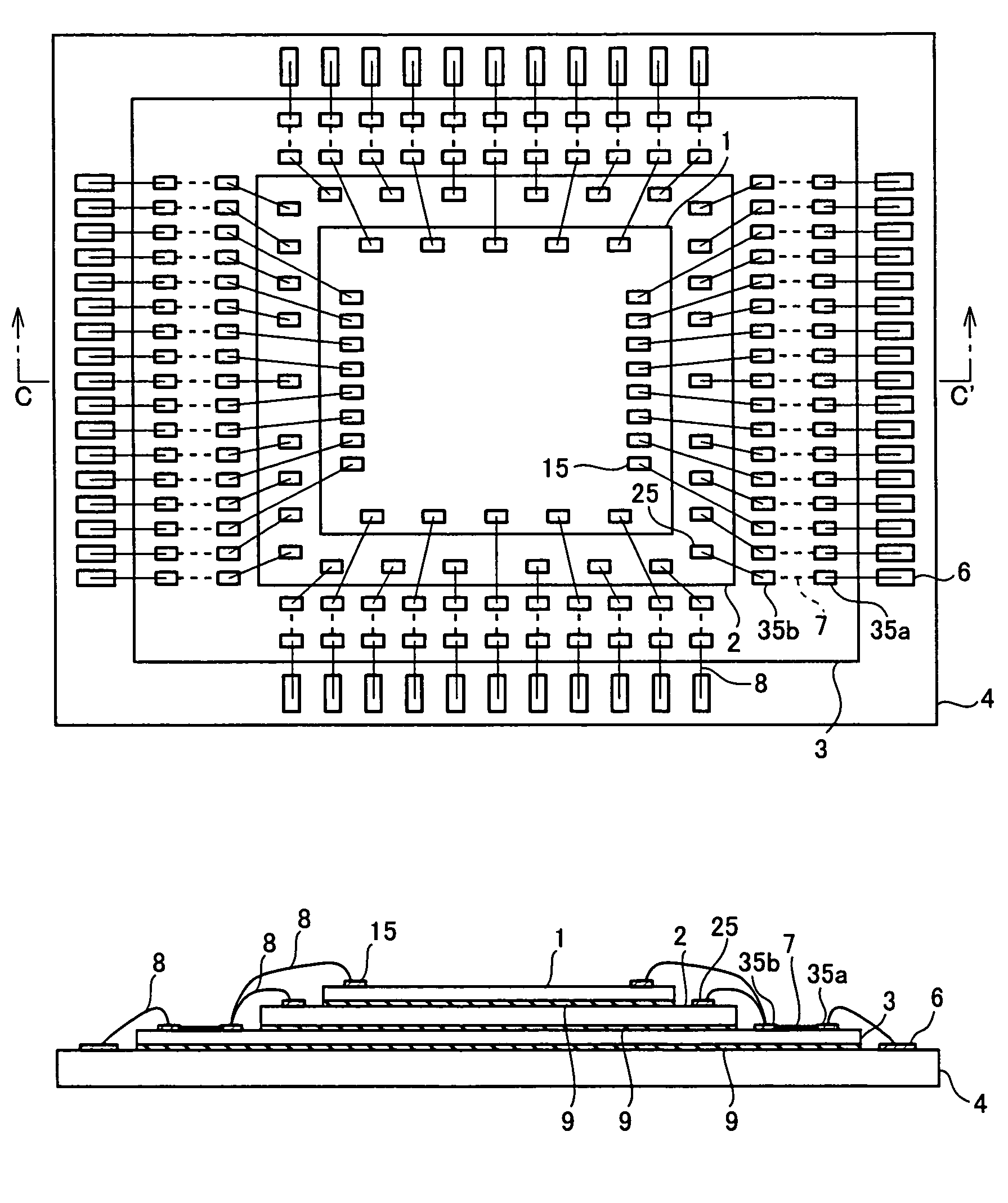
[0072]The following description will explain still another embodiment of the semiconductor device of the present invention with reference to FIG. 3(a) and FIG. 3(b). Note that, for convenience in description, the same reference signs are given to members having the same functions as members described in Embodiment 1, and description thereof is omitted.
[0073]FIG. 3(a) is a plan view obtained by viewing the semiconductor device of the present embodiment from above in a stacking direction, and FIG. 3(b) is a cross sectional view taken along C–C′ of FIG. 3(a). As shown in FIG. 3(a) and FIG. 3(b), the semiconductor device of the present embodiment is arranged so that: the interposer chip 3 is stacked on an upper surface of the substrate 4, and the semiconductor chips 1 and 2 are stacked thereon and thereabove in this order. That is, in the present embodiment, the interposer chip 3 is formed between the substrate 4 and the semiconductor chip 2.
[0074]The bonding pads 15 . . ....
PUM
Abstract
In a semiconductor device in which a semiconductorchip is stacked on a substrate, an interposerchip having wirings is provided under the semiconductorchip. A bonding pad of the semiconductor chip is electrically connected to a bonding terminal provided on the substrate via the interposer chip by wire bonding. The interposer chip prevents a semiconductor element formed in the semiconductor chip from deteriorating in terms of an electric property and from being physically damaged. Further, the wire bonding strength does not drop. Moreover, it is possible to form a fine wiring pitch for relaying a wire-bonding wire.
Description
[0001]This Nonprovisional application claims priority under 35 U.S.C. §119(a) on Patent Application No. 2003 / 020971 filed in Japan on Jan. 29, 2003, the entire contents of which are hereby incorporated by reference.FIELD OF THE INVENTION[0002]The present invention relates to a semiconductor device, particularly, to a semiconductor device in which a plurality of semiconductor chips are stacked.BACKGROUND OF THE INVENTION[0003]In order to realize high-density installation of semiconductor chips which is a key technology for making an electronic device smaller, lighter, and thinner, various packaging techniques of a semiconductor device have been developed.[0004]As a technique concerning a packaging structure of a semiconductor device which reduces an area required in installing the semiconductor device onto a mother board, there have been developed: a pin-insert package such as DIP (Dual Inline Package); a surface installation package, such as SOP (Small Outline Package), performed by...
Claims
Application Information
Patent Timeline
Application Date:The date an application was filed.
Publication Date:The date a patent or application was officially published.
First Publication Date:The earliest publication date of a patent with the same application number.
Issue Date:Publication date of the patent grant document.
PCT Entry Date:The Entry date of PCT National Phase.
Estimated Expiry Date:The statutory expiry date of a patent right according to the Patent Law, and it is the longest term of protection that the patent right can achieve without the termination of the patent right due to other reasons(Term extension factor has been taken into account ).
Invalid Date:Actual expiry date is based on effective date or publication date of legal transaction data of invalid patent.

