

Test interconnect for bumped semiconductor components and method of fabrication
a technology of bumped semiconductor components and interconnections, which is applied in the direction of individual semiconductor device testing, printed element electric connection formation, instruments, etc., can solve the problems of easy deformation of contacts during handling, difficulty in reliable electrical connection, and different sizes of bumped contacts on a componen
- Summary
- Abstract
- Description
- Claims
- Application Information
AI Technical Summary
Benefits of technology
Problems solved by technology
Method used
Image

Examples
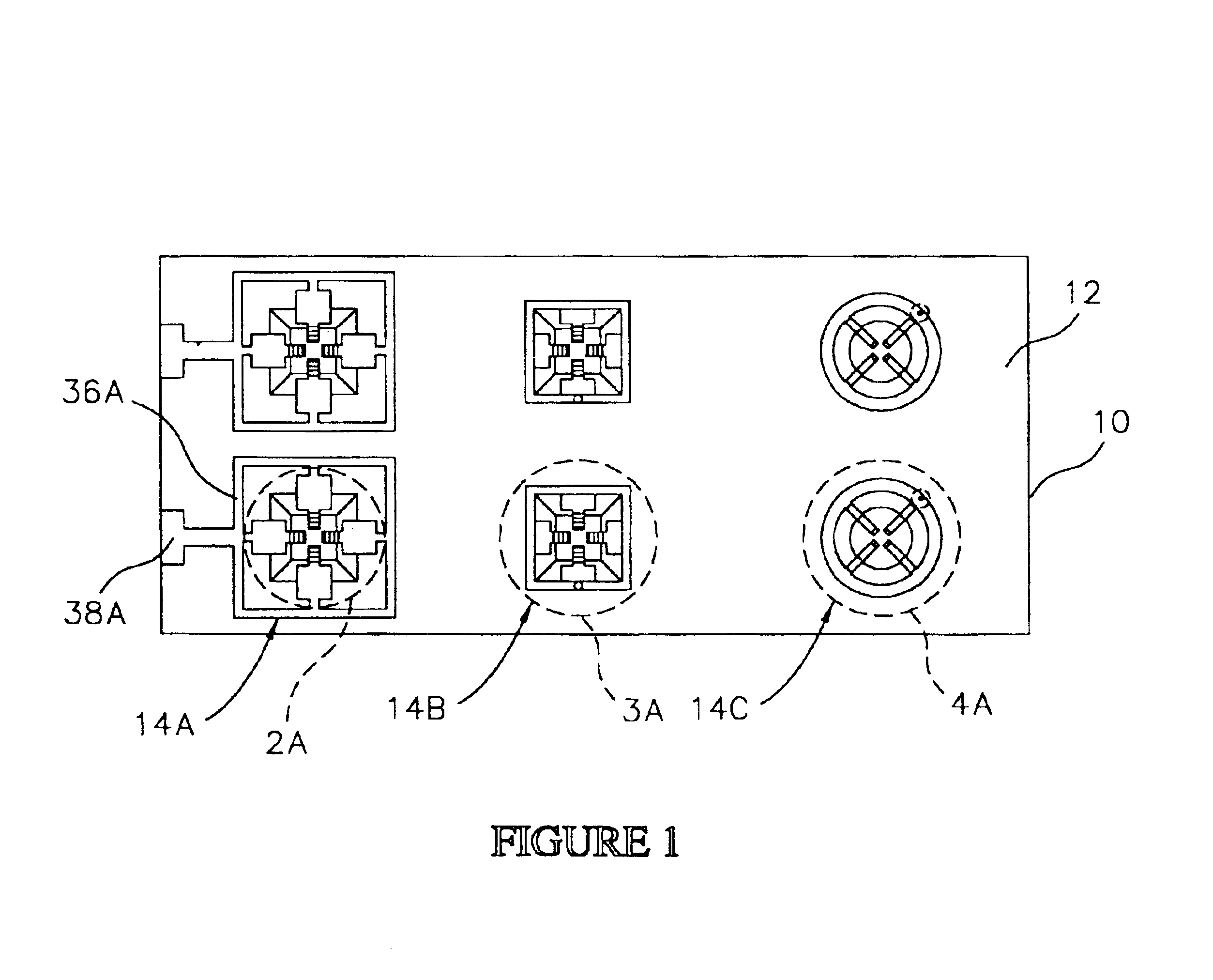
first embodiment
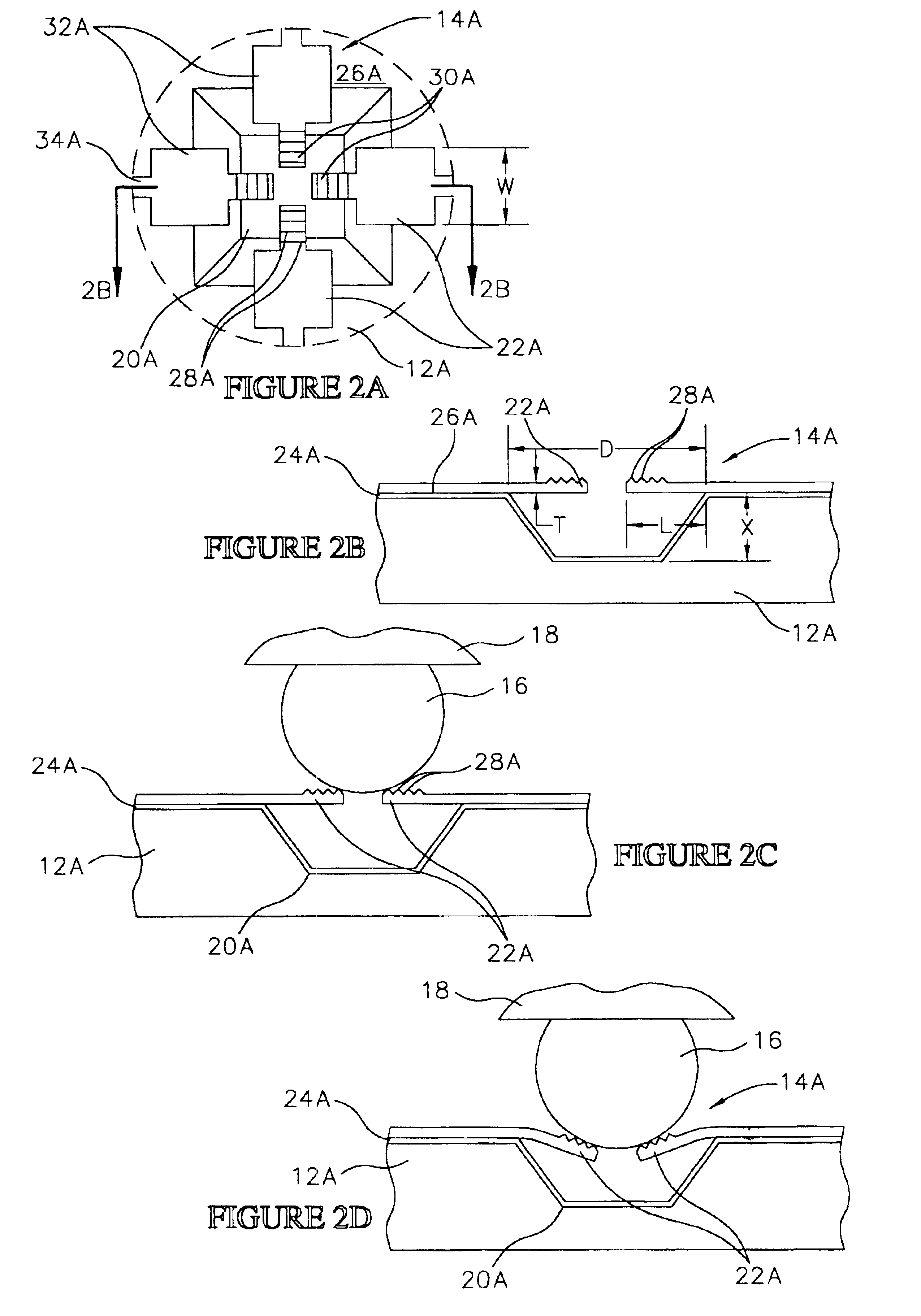
[0050]Referring to FIGS. 2A-2C, the first embodiment contact 14A comprises a recess 20A in a substrate 12A, and a plurality of metal leads 22A cantilevered over the recess 20A. The recess 20A and leads 22A are sized and shaped to compensate for variations in the size (e.g., diameter, height), shape, and planarity of the bumped contacts 16 (FIG. 2C) on the component 18 (FIG. 2C).
[0051]The substrate 12A can comprise a semiconductor material such as monocrystalline silicon, germanium, silicon-on-glass, or silicon-on-sapphire. In addition, an electrically insulating layer 24A (FIG. 2B) can be formed on a surface 26A of the substrate 12A and within the recess 20A for electrically insulating the contact 14A from a bulk of the substrate 12A. However, as will be further explained the substrate can also comprise an electrically insulating material, such as ceramic or plastic, such that electrically insulating layers are not be required.
[0052]The recess 20A can be formed in the substrate 12A ...
second embodiment
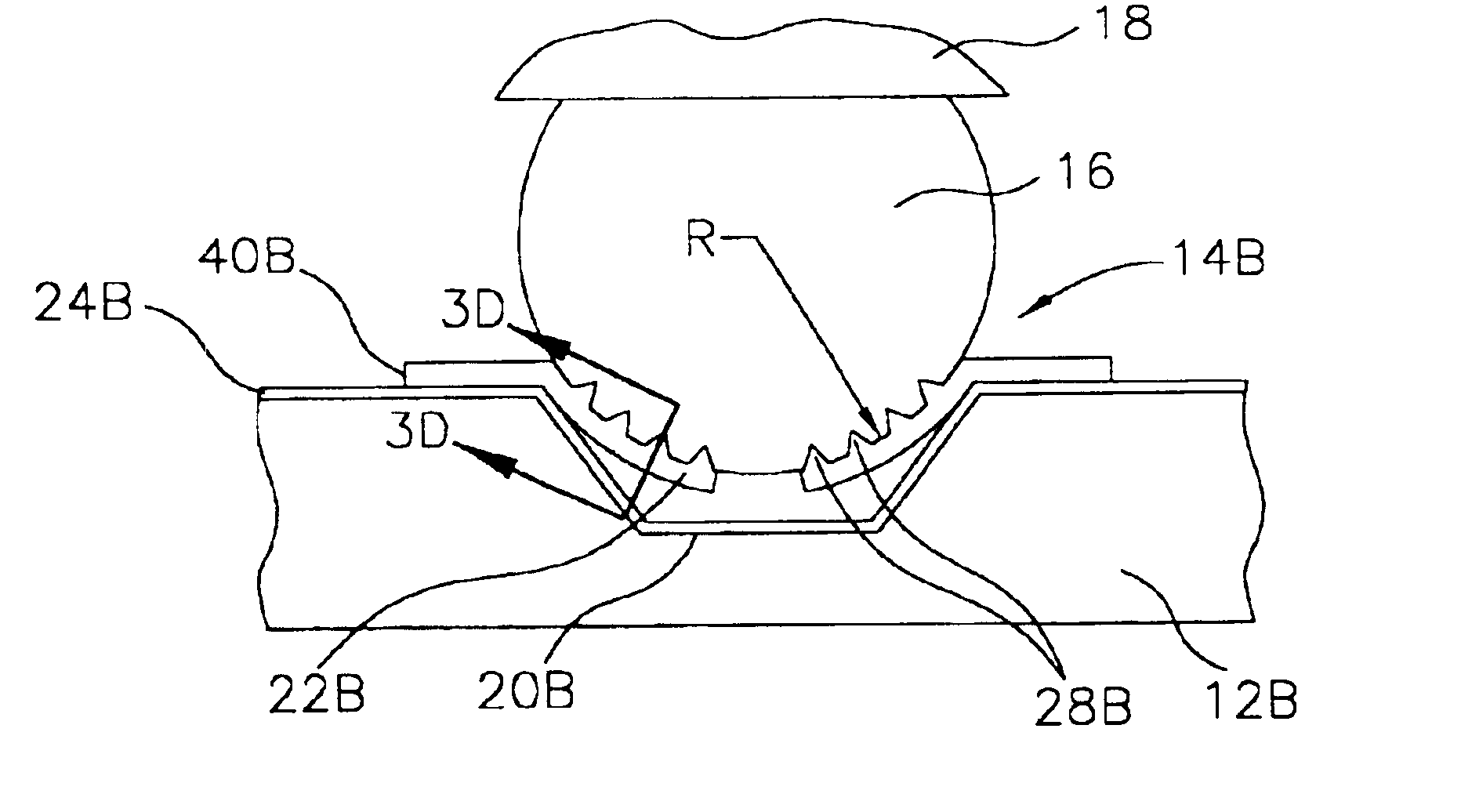
[0060]Referring to FIGS. 3A-3D, the second embodiment contact 14B is illustrated. The contact 14B comprises a recess 20B formed in a substrate 14B, substantially as previously described. In addition, the contact 14B comprises a plurality of leads 22B cantilevered over the recess 20B, and having blades 28B for penetrating the contact bumps 16 substantially as previously described. However, in this embodiment the leads 22B have a curved shape that substantially matches a shape of the outer surface of the bumped contacts 16. Specifically the leads 22B have a radius of curvature R approximately equal to a radius of the bumped contacts 16. As with the previous embodiment, the leads 22B are configured to flex in the z-direction within the recess 20B to compensate for variations in the size or planarity of the bumped contacts 16.
[0061]The contact 14B also includes a conductive connecting segment 40B for electrically interconnecting the leads 22B. The conductive connecting segment 40B compr...
third embodiment
[0063]Referring to FIGS. 4A-4C, the third embodiment contact 14C is illustrated. The contact 14C comprises: a substrate 12C; a recess 20C formed in the substrate 12C; and conductive beams 48C cantilevered over the recess 20C.
[0064]The recess 20C has a generally circular peripheral configuration and can be formed using an etch process substantially as previously described. In addition, the conductive beams 48C can be formed integrally with the substrate 12C using an etching process to be hereinafter described. As with the leads 22A (FIG. 2B), a length, thickness, width, and modulus of elasticity of the conductive beams 48C can be selected to provide a desired spring constant.
[0065]The conductive beams 48C are at least partially covered with metal layers 50C. The metal layers 50C are electrically interconnected by a connecting segment 40C on a surface 26C of the substrate 12C which encircles a periphery of the recess 20C. In addition, the metal layers 50C are in electrical communicati...
PUM
| Property | Measurement | Unit |
|---|---|---|
| diameter | aaaaa | aaaaa |
| depth | aaaaa | aaaaa |
| temperature | aaaaa | aaaaa |
Abstract
Description
Claims
Application Information