Printable electronic display

a printing and electronic display technology, applied in the field of electronic displays, can solve the problems of relatively poor manufacturing yield, high production cost, and relatively complex and costly fabrication, and achieve the effects of facilitating addressing, reducing cost, and facilitating fabrication

Inactive Publication Date: 2005-12-27
MASSACHUSETTS INST OF TECH
View PDF73 Cites 254 Cited by
  • Summary
  • Abstract
  • Description
  • Claims
  • Application Information

AI Technical Summary

Benefits of technology

[0009]The present invention facilitates fabrication of an entire nonemissive (reflective), electronically addressable display using printing techniques. In particular, printing processes can be used to deposit the electrodes, insulating material, the display itself, and an array of nonlinear devices to facilitate addressing. Accordingly, fabrication of the displays of the present invention may be accomplished at significantly lower cost and with far less complexity than would obtain using coventional fabrication technologies. Furthermore, the approach of the present invention affords greater versatility in fabrication, allowing the displays to be applied to substrates of arbitrary flexibility and thickness (ranging, for example, from polymeric materials to paper). For example, static screen-printed displays may be used in signs or lettering on consumer products; the invention can also be used to form dynamic, electronically alterable displays. Moreover, the invention can be employed to produce flat-panel displays at manufacturing costs well below those associated with traditional devices (e.g., liquid crystal displays).

Problems solved by technology

Again, these materials have traditionally been applied using costly sputtering or vacuum deposition methods.
While these types of devices achieve the desired result, both involve thin-film processes.
Thus they suffer from high production cost as well as relatively poor manufacturing yields.
Thus, fabrication is relatively complex and costly.
These displays, however, have for the most part been emissive in nature (such as electroluminescent displays).
As is well known, emissive displays exhibit high power-consumption levels.
Efforts devoted to nonemissive displays generally have not provided for thresholding to facilitate matrix addressing.

Method used


Image

  • Printable electronic display
  • Printable electronic display
  • Printable electronic display

Examples


Embodiment Construction

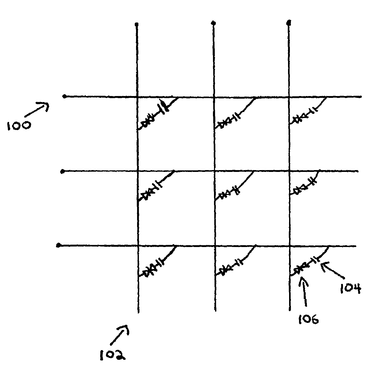
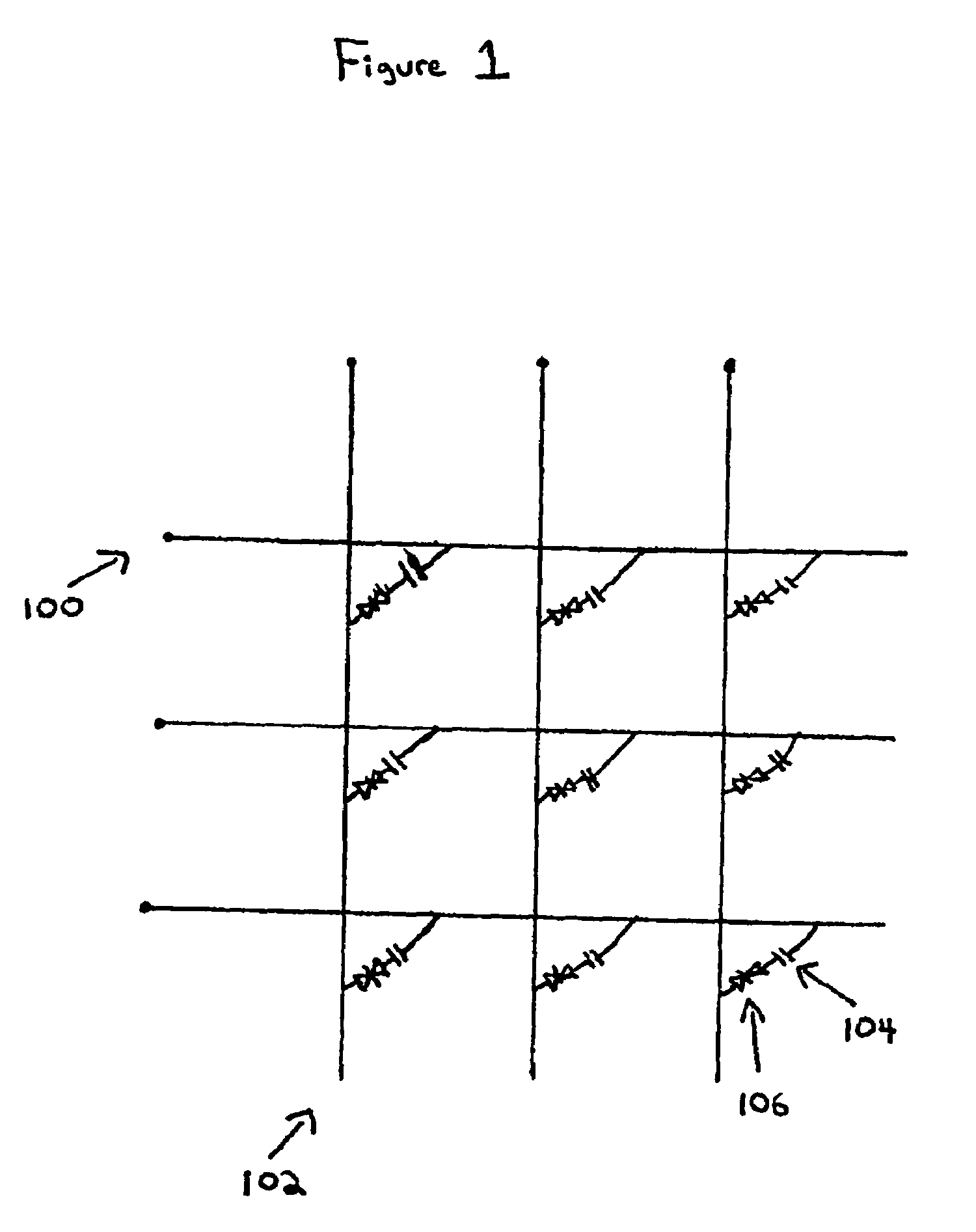
[0031]Refer first to FIG. 1, which schematically illustrates a display system in accordance with the invention. The depicted system includes an electrophoretic display, and the various components are deposited by a printing process as permitted by the present invention. It should be understood, however, that the invention may be practiced using other particle-based displays, and with components deposited by conventional (e.g., vacuum-type) processes.

[0032]The illustrated embodiment includes a series of row and column electrodes indicated generally at 100 and 102, respectively, and preferably formed using a printed conductive ink. Assuming the column electrodes 100 are the ones through which the display is viewed, these are transparent. The row electrodes 102, which serve as the rear electrodes, may or may not be transparent, depending upon the application. The electrophoretic display material 104 and the nonlinear elements 106 are sandwiched between column electrodes 100 and row ele...


PUM

PropertyMeasurementUnit
temperatureaaaaaaaaaa
temperaturesaaaaaaaaaa

Abstract

A display system includes a substrate upon which the display system is fabricated; a printable electrooptic display material, such as a microencapsulated electrophoretic suspension; electrodes (typically based on a transparent, conductive ink) arranged in an intersecting pattern to allow specific elements or regions of the display material to be addressed; insulating layers, as necessary, deposited by printing; and an array of nonlinear elements that facilitate matrix addressing. The nonlinear devices may include printed, particulate Schottky diodes, particulate PN diodes, particulate varistor material, silicon films formed by chemical reduction, or polymer semiconductor films. All elements of the display system may be deposited using a printing process.

Description

FIELD OF THE INVENTION[0001]The present invention relates to electronic displays, and in particular to non-emissive, flat-panel displays.BACKGROUND OF THE INVENTION[0002]Electrooptic display systems typically include an electrooptic element (e.g., the display material itself) and electrodes (either opaque or transparent) for applying control voltages to the electrooptic element. Such a system may also include a nonlinear element to allow for multiplexing of the address lines to the electrodes, and an insulating material between various layers of the display system. These components have been fabricated by a multitude of conventional processes. For versatility and convenience of manufacture, many recent efforts have focused on producing all components of such displays by deposition printing using, for example, screen or ink-jet printing apparatus. The use of printing techniques allows displays to be fabricated on a variety of substrates at low cost.[0003]The conducting materials used...

Claims


Application Information

Patent Timeline
Patent Type & Authority Patents(United States)
IPC IPC(8): G02F1/1365G02F1/167G02F1/16757G02F1/16766G02F1/1679H02J17/00
CPCG02F1/1365G02F1/167G02F1/172G02F1/16757G02F1/1679G02F1/16766
Inventor TURNER, CHRISTOPHERJACOBSON, JOSEPH M.COMISKEY, BARRETT
Owner MASSACHUSETTS INST OF TECH
Why Eureka
Try Eureka