Memory cell architecture for reduced routing congestion

a memory cell and routing technology, applied in semiconductor devices, digital storage, instruments, etc., can solve the problems of capacitive memory cells not maintaining their contents, ram storage is generally volatile, and leakage currents within semiconductor memory are unavoidable, so as to reduce the effect of consuming a small amount of space, reducing the effect of effect and minimizing the

Active Publication Date: 2005-12-27
AVAGO TECH INT SALES PTE LTD
View PDF1 Cites 54 Cited by
  • Summary
  • Abstract
  • Description
  • Claims
  • Application Information

AI Technical Summary

Benefits of technology

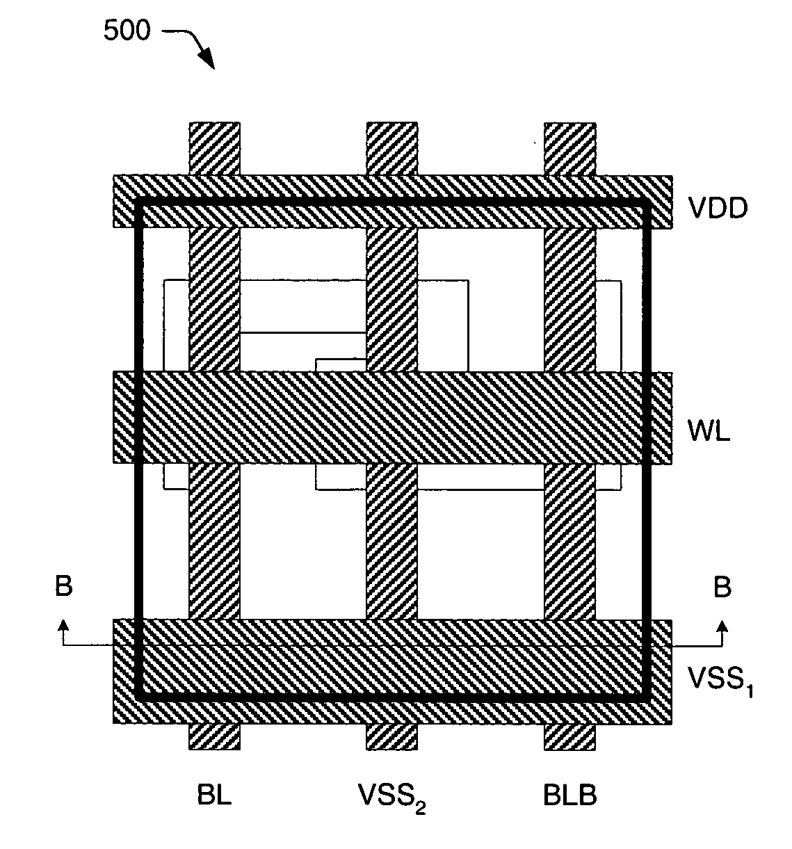
[0019]The problems outlined above may be in large part addressed by an improved memory cell architecture capable of reducing, or altogether eliminating, chip-level routing congestion in System-on-Chip environments. Though only a few embodiments are provided herein, features common to the described embodiments include: the formation of bitlines in a lower-level metallization layer of the memory array, and the use of word lines and ground supply lines, both formed in inter-level metallization layer(s) of the memory array, for effective shielding of the bitlines against routing signals in an upper-level metallization layer.
[0024]In any case, the intrinsic capacitance of the bitlines may be minimized by forming the bitlines within the lowest metal layer (e.g., the first or second metal layer) available within the memory cell. In some cases, the lowest metal layer may be dependent on the type of memory cell, as well as the process technology used to fabricate the memory cell. A significant improvement in speed and performance is attained by forming the bitlines within the lowest available metal layer of the memory cell.
[0028]In one configuration of the memory array, the second plurality of global ground supply lines may be formed within the second metal layer. Such a configuration may substantially eliminate routing congestion within the fourth metal layer, while minimizing voltage fluctuations on a selected one of the first plurality of global ground supply lines (i.e., the VSS1 line associated with an asserted row during a read operation). Such a configuration may also provide horizontal shielding between bitlines of dissimilar ports, if the memory array comprises memory cells with more than one port.
[0029]In another configuration of the memory array, the second plurality of global ground supply lines may be formed within the fourth metal layer. Such a configuration may reduce routing congestion within the fourth metal layer, while minimizing voltage fluctuations on the selected one of the first plurality of global ground supply lines. Such a configuration may also minimize an amount of area consumed by the memory array.
[0033]In one configuration of the system, the second plurality of global ground supply lines may be formed, along with the plurality of bitlines, within a lower-level metallization layer of the system, where the lower-level metallization layer is arranged below the inter-level metallization layer. In some cases, at least one of the first plurality and at least one of the second plurality of global ground supply lines may be formed within each row of memory cells. Such a configuration may substantially eliminate routing congestion within the upper-level metallization layer, while minimizing the effects of voltage droop, ground bounce and electromigration. Such a configuration may also provide horizontal capacitive shielding between bitlines of dissimilar ports, if the memory array comprises memory cells of more than one port.
[0034]In another configuration of the system, the second plurality of global ground supply lines may be formed, along with the plurality of transmission lines, within the upper-level metallization layer of the system. In some cases, at least one of the first plurality of global ground supply lines may be formed within each row of memory cells; however, each of the second plurality of global ground supply lines may be shared by two or more rows of memory cells. In addition to the effects of voltage droop, ground bounce and electromigration, such a configuration may minimize an amount of area consumed by the system, while reducing routing congestion within the upper-level metallization layer.

Problems solved by technology

On the other hand, RAM storage is generally volatile, and must remain powered-up in order to preserve its contents.
The first of these is that leakage currents within the semiconductor memory are unavoidable, and act to limit the length of time the memory cell capacitors can hold their charge.
Otherwise, the capacitive memory cells would not maintain their contents.
Secondly, changing the state of a DRAM memory cell requires charging or discharging the cell capacitor.
The time required to do this depends on the amount of current the transistor-based buffer can source or sink, but generally cannot be done as quickly as a bistable latch can change state.
Therefore, DRAMs are typically slower than SRAMs.
Unfortunately, many of these SoC designs suffer from data corruption, which may be caused by stray capacitances from chip-level signals routed over the memory blocks.
Though strict routing restrictions may be imposed to avoid data corruption, such restrictions often lead to chip-level routing congestion and undesirable increases in overall chip area.

Method used


Image

  • Memory cell architecture for reduced routing congestion
  • Memory cell architecture for reduced routing congestion
  • Memory cell architecture for reduced routing congestion

Examples


Embodiment Construction

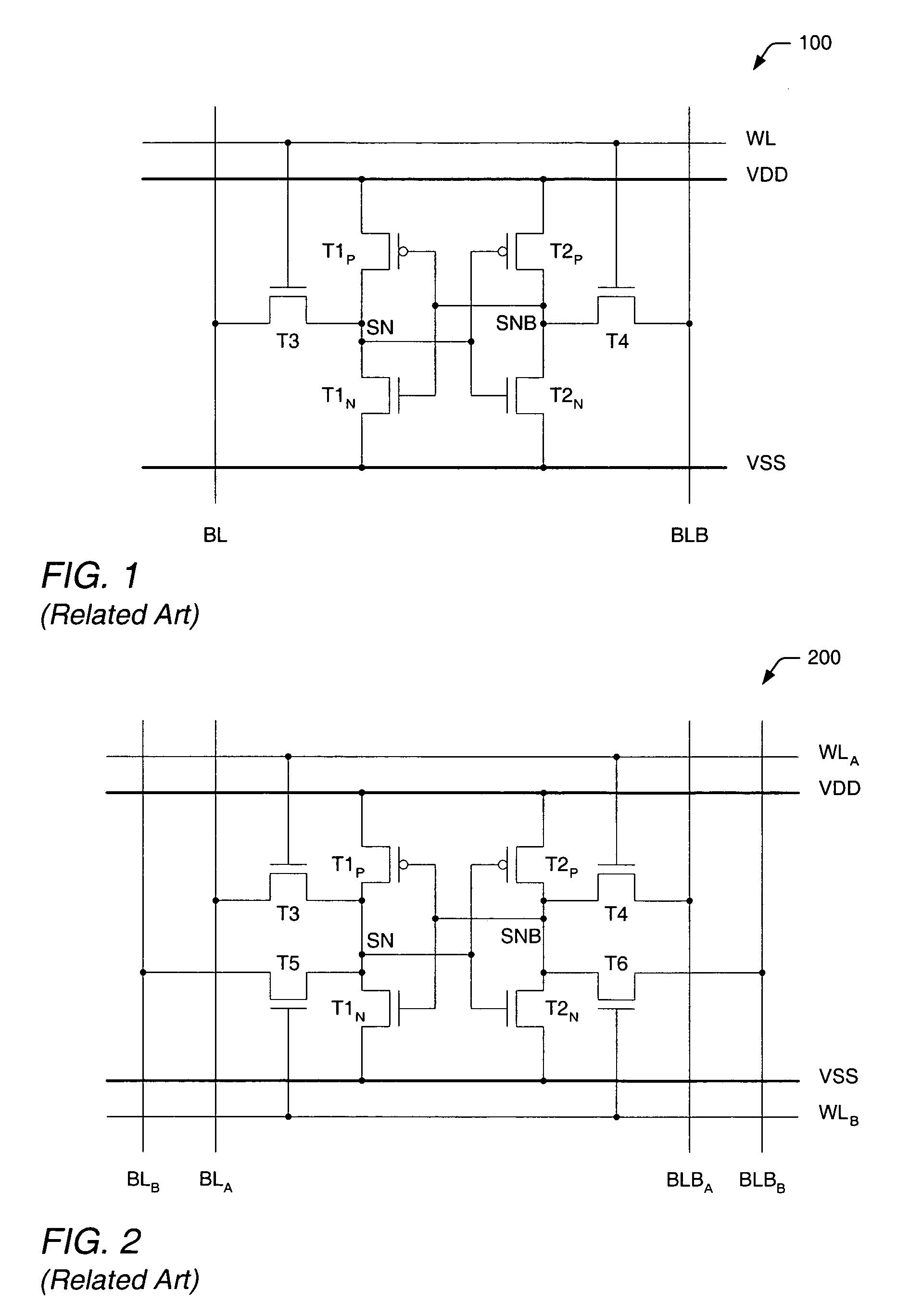
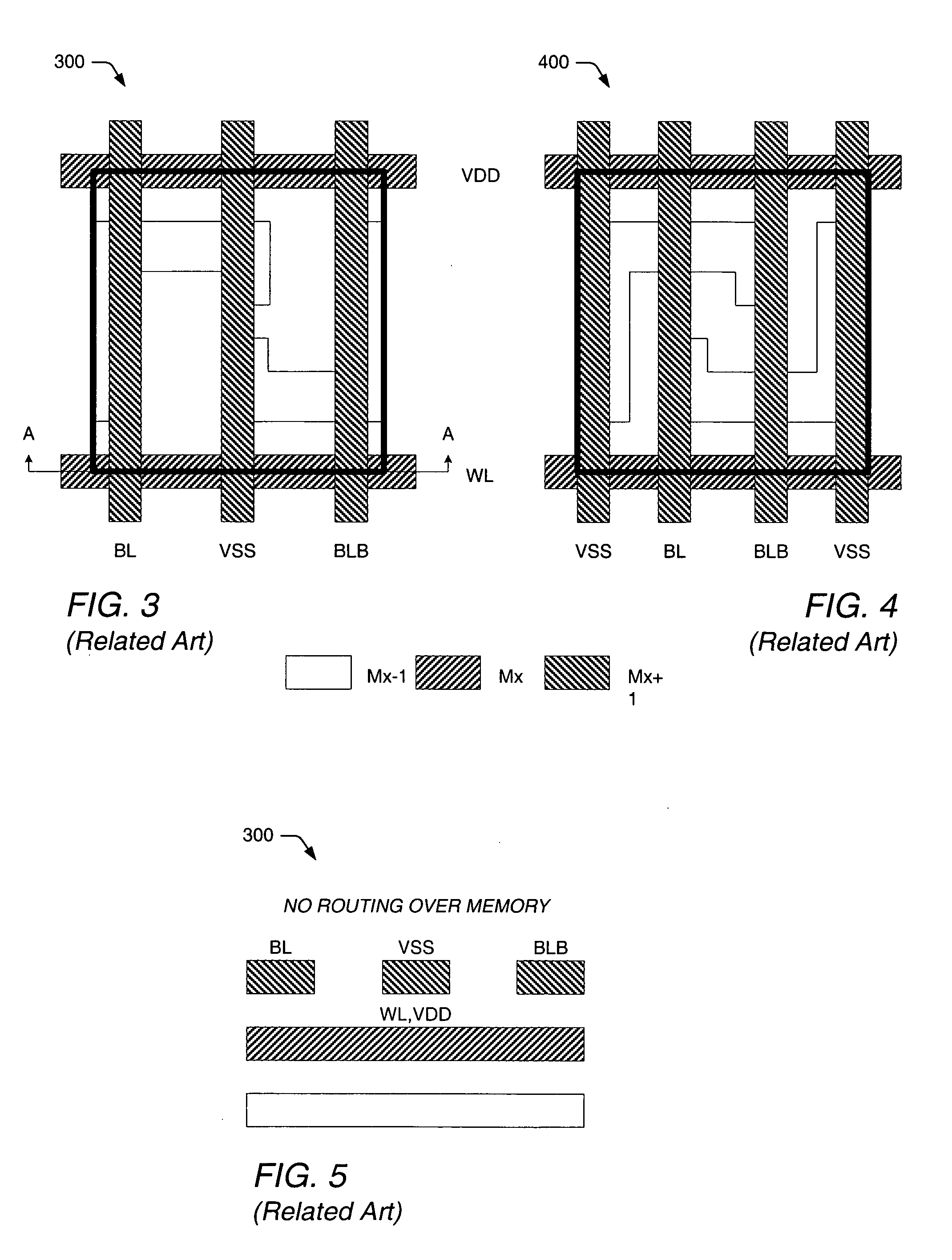
[0051]FIGS. 3–5 illustrate exemplary embodiments of a cell architecture that may be used to form a single-port SRAM cell, such as memory cell 100 of FIG. 1. FIGS. 3 and 4 present top-down views of cell architectures 300 and 400, respectively. FIG. 5 presents a cross-sectional view along line AA of cell architecture 300. Though the architecture of only one memory cell is illustrated in FIGS. 3–5, and later in FIGS. 6–9, one of ordinary skill in the art would understand how the architecture could be applied to an array of memory cells.

[0052]In most SRAM architectures, including those illustrated in FIGS. 3–5, the bitlines and wordlines of the memory cell run orthogonal to one another on separate metallization layers. Therefore, at least two metallization layers are needed to form an SRAM cell. In some cases, more than two metallization layers may be used in an effort to increase cell density by decreasing the cell aspect ratio. In general, the term “aspect ratio” is used herein to des...


PUM


Abstract

An improved memory cell architecture is provided herein for reducing, or altogether eliminating, chip-level routing congestion in System-on-Chip environments. Though only a few embodiments are provided herein, features common to the described embodiments include: the formation of bitlines in a lower-level metallization layer of the memory array, and the use of word lines and ground supply lines, both formed in inter-level metallization layer(s) of the memory array, for effective shielding of the bitlines against routing signals in the chip-level routing layer.

Description

BACKGROUND OF THE INVENTION[0001]1. Field of the Invention[0002]This invention relates to semiconductor integrated devices and, more particularly, to semiconductor memory devices having reduced routing congestion within upper level metallization layers.[0003]2. Description of the Related Art[0004]The following descriptions and examples are not admitted to be prior art by virtue of their inclusion within this section.[0005]Generally speaking, system-on-chip (SoC) technology is the ability to place multiple function “subsystems” on a single semiconductor chip. The term “system-on-chip” may be used to describe many of today's complex ASICs, where many functions previously achieved by combining multiple chips on a board are now provided by one single chip. SoC technology provides the advantages of cutting development cycle time, while increasing product functionality, performance and quality. The various types of subsystems that may be integrated within the semiconductor chip include mi...

Claims


Application Information

Patent Timeline
Patent Type & Authority Patents(United States)
IPC IPC(8): G11C5/06G11C11/00H01L27/02H01L27/105H01L27/118
CPCG11C5/063H01L27/0207H01L27/105H01L27/11807
Inventor RAMESH, SUBRAMANIANCASTAGNETTI, RUGGEROVENKATRAMAN, RAMNATH
Owner AVAGO TECH INT SALES PTE LTD
Why Eureka
Try Eureka