Semiconductor device having a vertical type semiconductor element

a vertical type, semiconductor technology, applied in the direction of semiconductor devices, basic electric elements, electrical appliances, etc., can solve the problem of performance exceeding the limit performance of silicon, and achieve the effect of reducing the electric field and allowing for further improvement of the resistance to voltag

Inactive Publication Date: 2006-01-03
DENSO CORP
View PDF31 Cites 96 Cited by
  • Summary
  • Abstract
  • Description
  • Claims
  • Application Information

AI Technical Summary

Benefits of technology

[0009]According to an aspect of the present invention, a depletion layer can be expanded toward the end portion in an inside of the super junction structure. Besides, at a side of the electrode portion in the super junction structure, the depletion layer can be expanded toward the end portion. With this structure, electric concentration can be loosened at the side of the electrode portion in the super junction structure, so that withstand voltage of the semiconductor device can be improved. As a result, according to the present invention, the withstand voltage exceeds the limit in silicon.
[0011]According to a second aspect of present invention, an inside of the semiconductor substrate is completely depleted by the super junction structure. Moreover, the electric field is decreased by expanding the depletion layer at the vicinity of a surface of the substrate. Therefore, the withstand voltage can be further improved.

Problems solved by technology

As a result, the performance exceeding the limit performance of silicon cannot be achieved.

Method used


Image

  • Semiconductor device having a vertical type semiconductor element
  • Semiconductor device having a vertical type semiconductor element
  • Semiconductor device having a vertical type semiconductor element

Examples


first embodiment

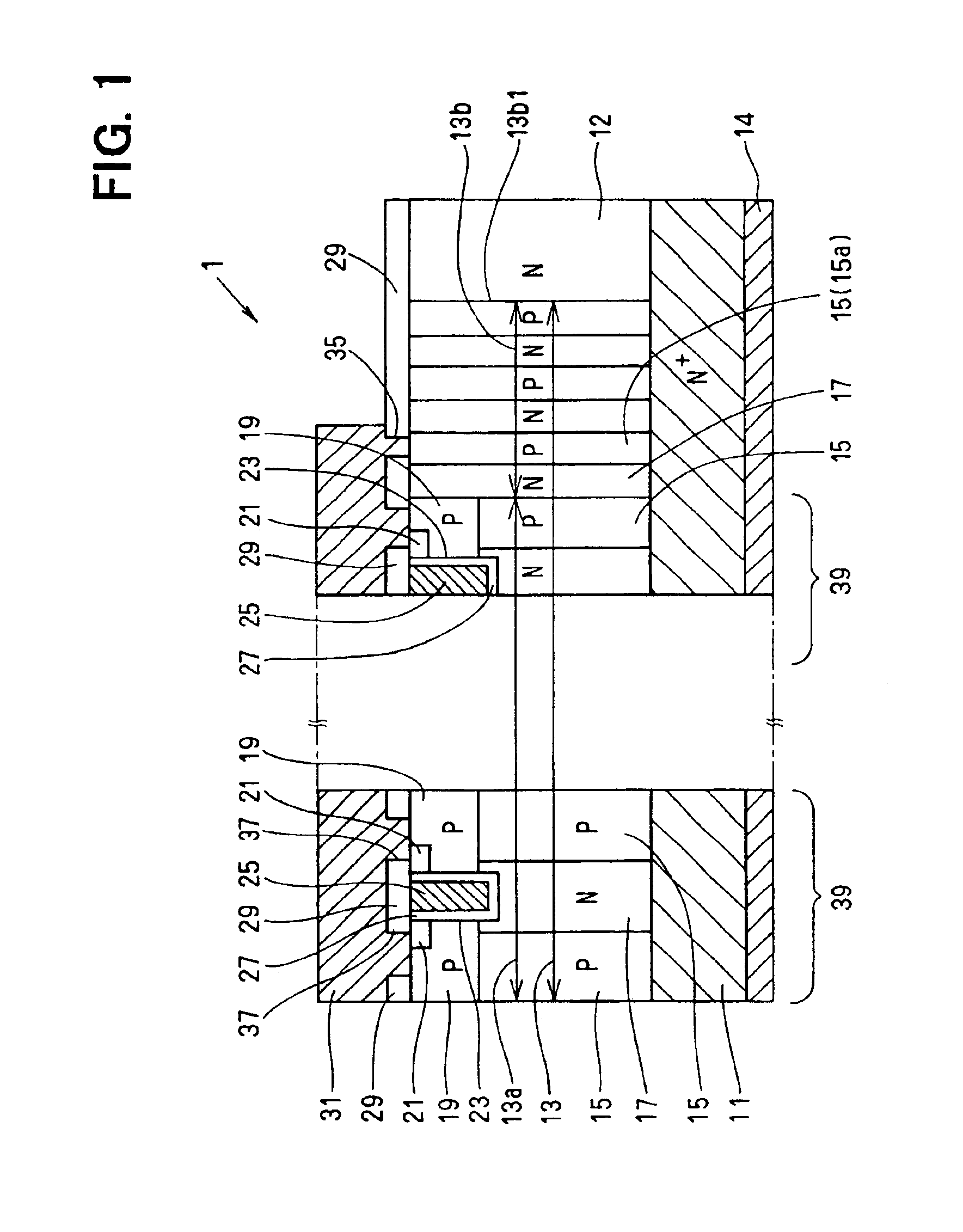
[0046]The present invention is employed to a vertical type MOS field effect transistor (hereinafter, referred to as a VMOS) 1 in this first embodiment. A schematic structure of the VMOS 1 will be explained below. A plurality of cells 39, i.e., a plurality of vertical type semiconductor elements constitutes the VMOS 1. Each cell 39 designates one unit in activation of the VMOS 1. Each of the plurality of cells 39 is arrayed in a transversal direction and a vertical (depth) direction with respect to the sheet of FIG. 1. A super junction structure 13 has a cell forming region 13a for the plurality of cells 39 and a peripheral region 13b that is located at a periphery of the cell forming region 13a. An electrode portion 31 is formed on a substrate as a source electrode so as to directly contact p-type regions and n-type regions as a source, and at least one of p-type regions in the peripheral region 13b. As a feature of the first embodiment, the electrode portion 31 is electrically cond...

second embodiment

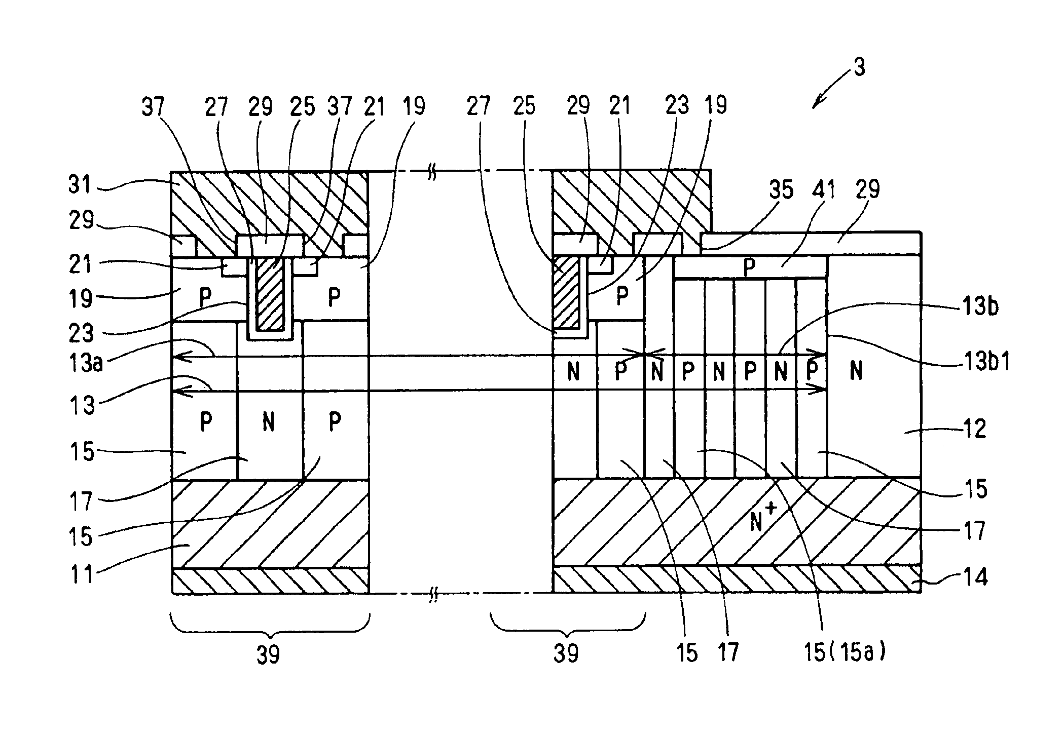
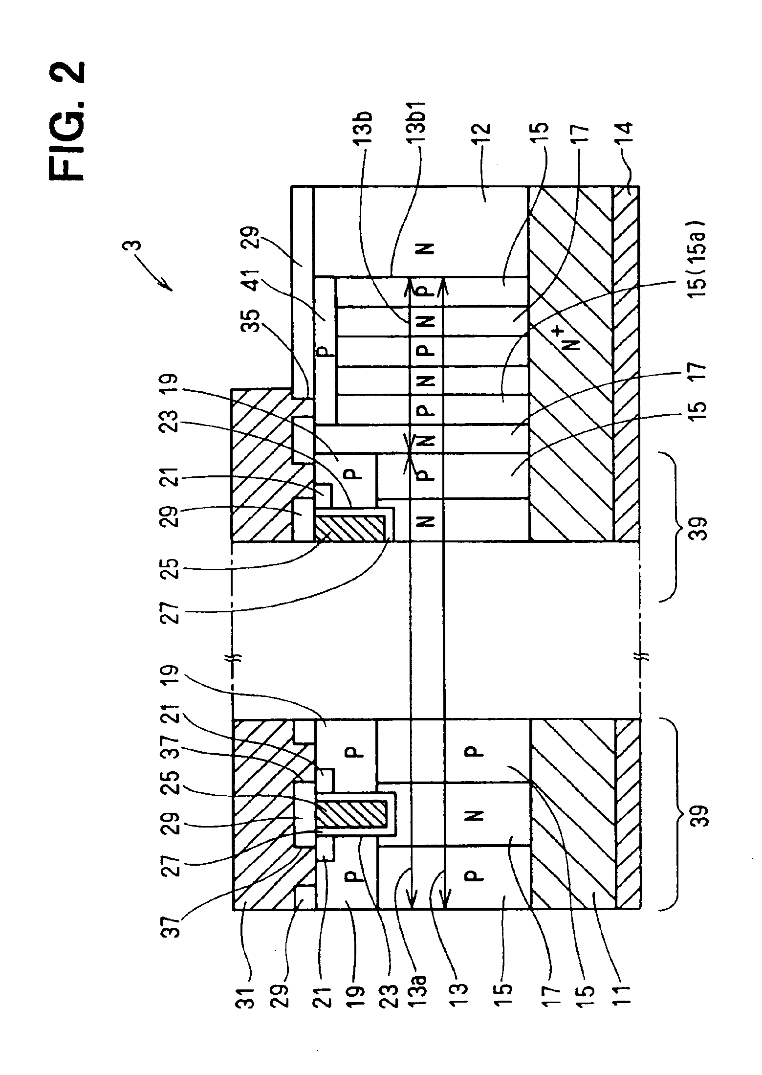
[0061]The present invention is employed to a vertical type MOS field effect transistor (hereinafter, referred to as a VMOS) 3 in this second embodiment. Portions in the VMOS 3 that are different from the VMOS 1 will be explained while explanation of the same or similar portions to the first embodiment will be omitted.

[0062]A P-type single crystal silicon region 41 is formed on the peripheral region 13b so as to be connected to the P-type single crystal silicon regions 15. Impurity concentration of the P-type single crystal silicon region 41 may be the same as the P-type single crystal silicon regions 15, or may be different from the P-type single crystal silicon regions 15. The electrode portion 31 is connected to the P-type single crystal silicon region 41 through the contact hole 35. According to the second embodiment, as explained in a simulation described below, the withstand voltage can be enhanced as compared to the first embodiment.

third embodiment

[0063]The present invention is employed to a vertical type MOS field effect transistor (hereinafter, referred to as a VMOS) 5 in this third embodiment. Portions in the VMOS 5 that are different from the VMOS 1 and VMOS 3 will be explained while explanation of the same or similar portions to the first embodiment will be omitted.

[0064]In the peripheral region, P-type single crystal silicon regions 15 are divided into an upper portion and a lower portion by an N-type single crystal silicon region 43, respectively. N-type single crystal silicon regions 17 are electrically conducted with each other through the N-type single crystal silicon regions 43. Impurity concentration of the N-type single crystal silicon regions 43 may be the same as the N-type single crystal silicon regions 17, or may be different from the N-type single crystal silicon regions 17. Hereinafter, a manufacturing method of the N-type single crystal silicon regions 43 will be described. The super junction structure 13 ...


PUM


Abstract

A vertical type MOS field effect transistor has a super junction structure between a source electrode and an N+-type drain region. The super junction structure is constituted by a plurality of P-type single crystal silicon regions and a plurality of N-type single crystal silicon regions. Each of the plurality of P-type single crystal silicon regions and each of the plurality of N-type single crystal silicon regions are arrayed alternately. The super junction has two parts, that is, a cell forming region where a MOS structure is disposed and a peripheral region located at a periphery of the cell forming region. The source electrode contacts one of the P-type single crystal silicon regions in the peripheral region while disposed away from an end portion of the peripheral region that is located at an outermost in the peripheral region.

Description

CROSS REFERENCE TO RELATED APPLICATION[0001]This application is a divisional of U.S. patent application Ser. No. 10 / 015,917, filed Dec. 17, 2001 now U.S. Pat. No. 6,639,260, which is based upon Japanese Patent Application No. 2000-383440 filed on Dec. 18, 2000, the contents of which are incorporated herein by reference.BACKGROUND OF THE INVENTION[0002]1. Field of the Invention[0003]The present invention relates to a semiconductor device which has a super junction structure.[0004]2. Related Art[0005]A vertical type MOS field effect transistor representing a vertical type semiconductor device is employed to, for example, a power conversion or a power control of a motor for a vehicle or household electric appliance. The one having a super junction structure is disclosed in JP-A-11-233759 and JP-A-9-266311. The super junction structure is constituted by a structure in which a first semiconductor region of first conductive type and a second semiconductor region of second conductive type ...

Claims


Application Information

Patent Timeline
Patent Type & Authority Patents(United States)
IPC IPC(8): H01L29/76H01L29/06H01L29/78
CPCH01L29/0634H01L29/7813H01L29/7811H01L29/0696
Inventor SUZUKI, TAKASHIUESUGI, TSUTOMUTOKURA, NORIHITO
Owner DENSO CORP
Why Eureka
Try Eureka