Self-aligned gate MOSFET with separate gates

a metal oxide semiconductor and gate technology, applied in the direction of semiconductors, electrical devices, transistors, etc., can solve the problems of difficult to make a low series resistance contact with the source/drain terminal, no satisfactory method of achieving self-alignment structure, and serious drawbacks in all of the above approaches

Inactive Publication Date: 2006-01-03
GLOBALFOUNDRIES INC
View PDF23 Cites 36 Cited by
  • Summary
  • Abstract
  • Description
  • Claims
  • Application Information

AI Technical Summary

Problems solved by technology

However, there is no satisfactory method of achieving this self-aligned structure.
There are serious drawbacks in all of the above approaches.
While in the vertical case (first), it is difficult to make a low series resistance contact to the source / drain terminal which is buried under the pillar.
In the third case, thickness control and top / bottom gate self-alignment are major problems.
In the fourth case, the control over the gate length is poor, and the two gates are electrically connected and must be made of the same material.
This may not be desirable in some applications for the following reasons.
Thus, this may impose a limitation on the process suggested in Chan.

Method used


Image

  • Self-aligned gate MOSFET with separate gates
  • Self-aligned gate MOSFET with separate gates
  • Self-aligned gate MOSFET with separate gates

Examples


Embodiment Construction

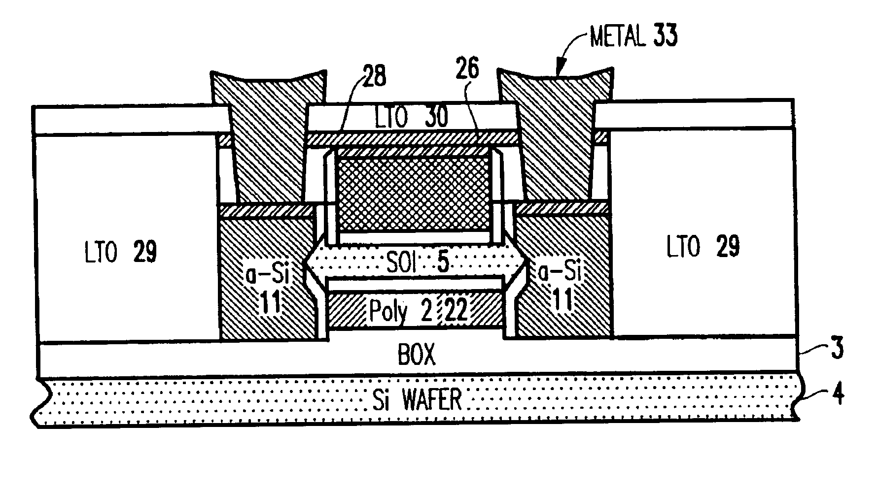
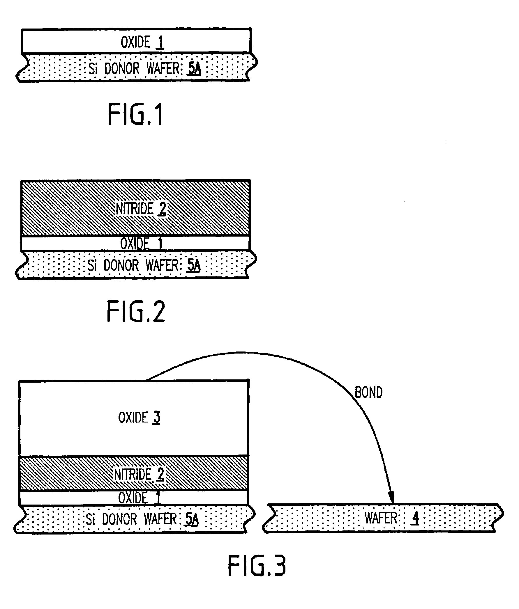
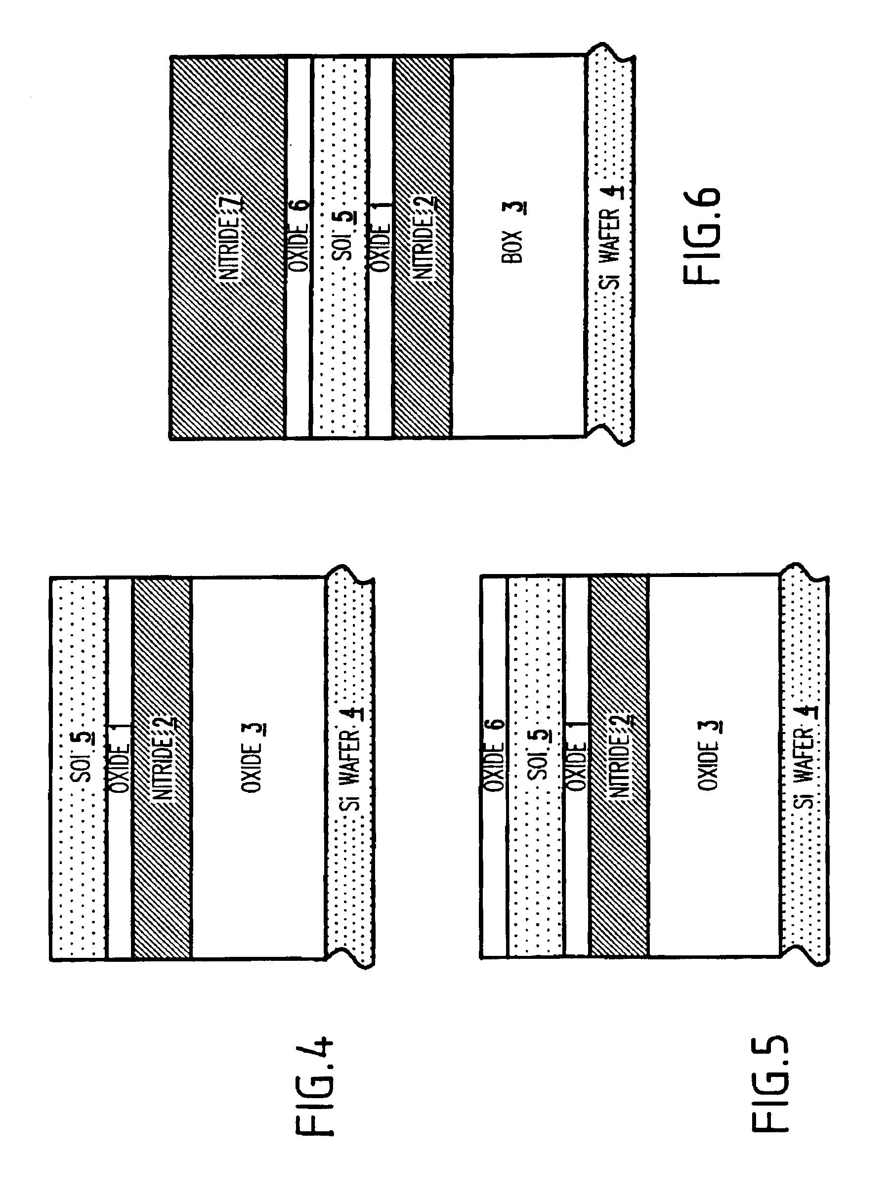
[0063]The following describes the present invention which is a self-aligned double-gate metal oxide semiconductor (DG-MOSFET), with electrically separated top and bottom gates and method for making the same. Moreover, the top and bottom gates comprise different materials.

[0064]As depicted in FIGS. 1-6, the invention begins by forming a series of layers. First, the invention forms a thin silicon dioxide 1 (e.g., about 2 nm thick) onto a single crystal wafer 5A, which is referred to as the donor wafer. Second, a layer of silicon nitride 2 (which can be, for example, approximately 100 nm thick) is formed onto the silicon dioxide layer 1. Third, a thick (e.g., approximately 400 nm) silicon dioxide layer 3 is formed onto the nitride layer 2. Fourth, the crystal wafer is bonded to a handle wafer 4. This bonding is performed using standard silicon wafer bonding techniques such as boron etch stop, smartCut, and other techniques well known to those skilled in the art (for a detailed discussi...


PUM


Abstract

A structure and method of manufacturing a double-gate integrated circuit which includes forming a laminated structure having a channel layer and first insulating layers on each side of the channel layer, forming openings in the laminated structure, forming drain and source regions in the openings, removing portions of the laminated structure to leave a first portion of the channel layer exposed, forming a first gate dielectric layer on the channel layer, forming a first gate electrode on the first gate dielectric layer, removing portions of the laminated structure to leave a second portion of the channel layer exposed, forming a second gate dielectric layer on the channel layer, forming a second gate electrode on the second gate dielectric layer, doping the drain and source regions, using self-aligned ion implantation, wherein the first gate electrode and the second gate electrode are formed independent of each other.

Description

BACKGROUND OF THE INVENTION[0001]1. Field of the Invention[0002]The present invention generally relates to a self-aligned double-gate metal oxide semiconductor (DG-MOSFET), with electrically separated top and bottom gates. Moreover, with the invention, the top and bottom gates may be formed by different materials.[0003]2. Description of the Related Art[0004]The double-gate metal oxide semiconductor field effect transistor (DG-MOSFET), is a MOSFET having a top and a bottom gate which control the carriers in the channel. The double-gate MOSFET has several advantages over a conventional single-gate MOSFET: higher transconductance, lower parasitic capacitance, avoidance of dopant fluctuation effects, and superior short-channel characteristics. Moreover, good short-channel characteristics are obtained down to 20 nm channel length with no doping needed in the channel region. This circumvents all the tunneling break-down, dopant quantization, and impurity scattering problems associated wit...

Claims


Application Information

Patent Timeline
Patent Type & Authority Patents(United States)
IPC IPC(8): H01L29/76H01L27/01H01L21/336H01L29/786
CPCH01L29/78648H01L29/66772
Inventor COHEN, GUY M.WONG, HON-SUM P.
Owner GLOBALFOUNDRIES INC
Why Eureka
Try Eureka