Nonvolatile ferroelectric memory device having a multi-bit control function

a ferroelectric memory and non-volatile technology, applied in the direction of information storage, static storage, digital storage, etc., can solve the problems of difficult to determine data, difficult to obtain a rapid operation speed of the feram chip having a b>1 and other problems, to achieve the effect of improving data access time and improving operation speed

Inactive Publication Date: 2006-01-03
SK HYNIX INC
View PDF11 Cites 6 Cited by
  • Summary
  • Abstract
  • Description
  • Claims
  • Application Information

AI Technical Summary

Benefits of technology

[0012]It is still another object of the present invention to embody a chip having an improved data access time by storing a plurality of read / written data through a register.
[0013]It is still another object of the present invention to secure the margin of a sensing voltage and improve the operation speed in the embodiment of a chip having a low voltage or a rapid access time by amplifying a self-sensing voltage of cell data in a reference timing interval and judging a plurality of voltage levels of data on a basis of a time axis.

Problems solved by technology

As a result, it is difficult to determine data.
Therefore, it is difficult to obtain a rapid operation speed of the FeRAM chip having a 1T1C (1transistor, 1capacitor).

Method used


Image

  • Nonvolatile ferroelectric memory device having a multi-bit control function
  • Nonvolatile ferroelectric memory device having a multi-bit control function
  • Nonvolatile ferroelectric memory device having a multi-bit control function

Examples


first embodiment

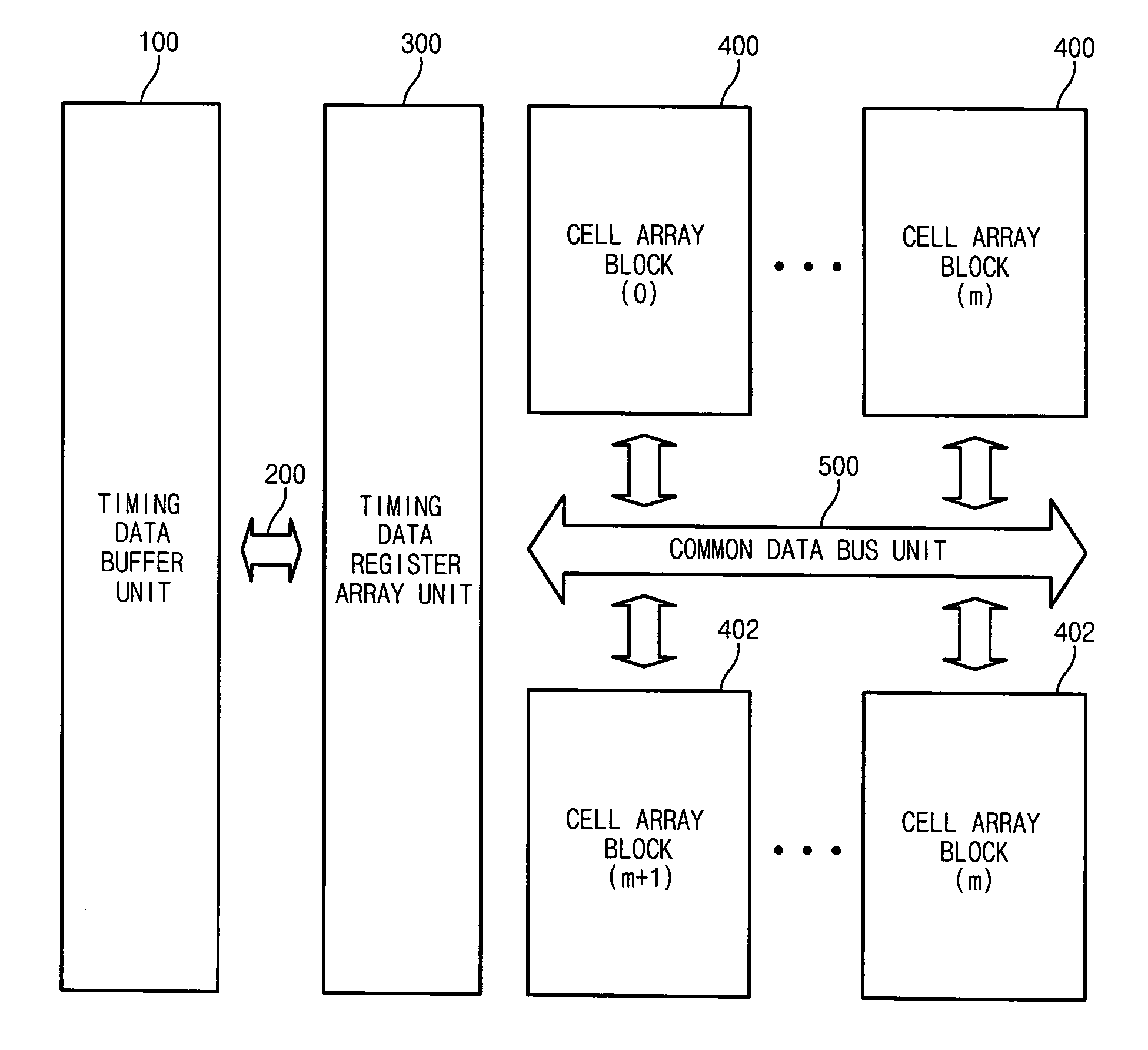
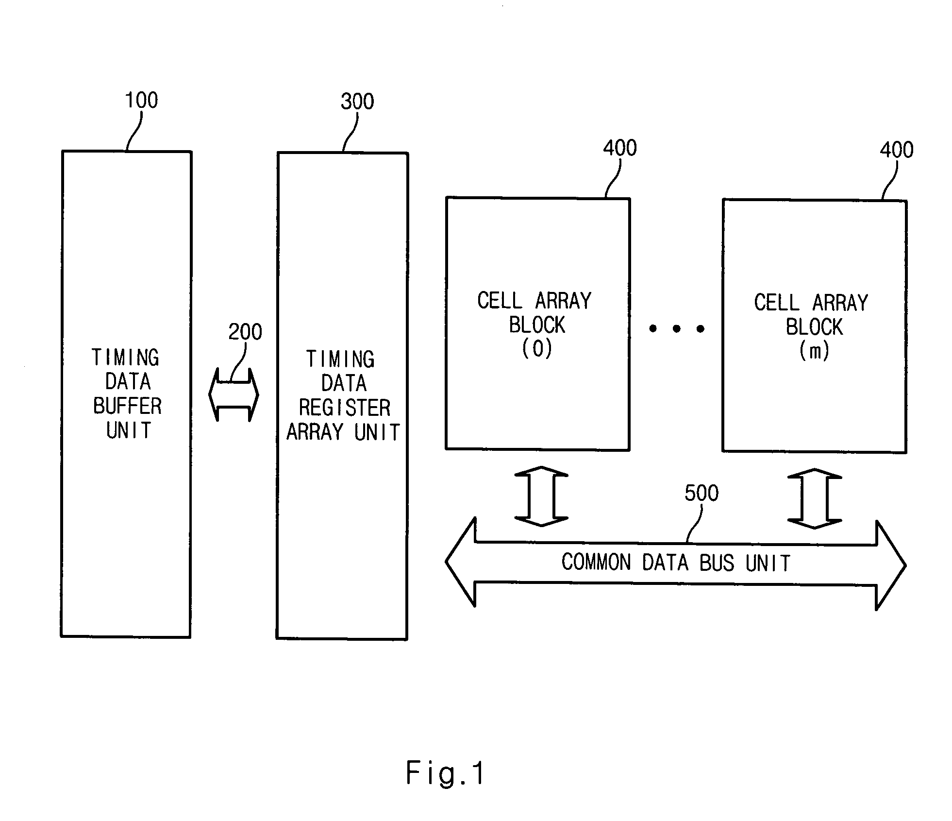
[0039]FIG. 1 is a diagram of a nonvolatile ferroelectric memory device having a multi-bit control function according to the present invention.

[0040]In an embodiment, the nonvolatile ferroelectric memory device comprises a timing data buffer unit 100, a data buffer bus unit 200, a timing data register array unit 300, a plurality of cell array blocks 400 and a common data bus unit 500.

[0041]The cell array block 400 comprises a plurality of cell arrays for storing data. The cell array block 400 comprises a bitline cell array having a multi-bitline structure comprising sub bitlines and a main bitline. The multi-bitline structure cell array converts a sensing voltage of the sub bitline into current, and induces a main bitline sensing voltage. Here, the plurality of cell array blocks 400 share the common data bus unit 500.

[0042]The timing data buffer unit 100 is connected to the timing data register array unit 300 through the data buffer bus unit 200. The timing data register array unit 3...

second embodiment

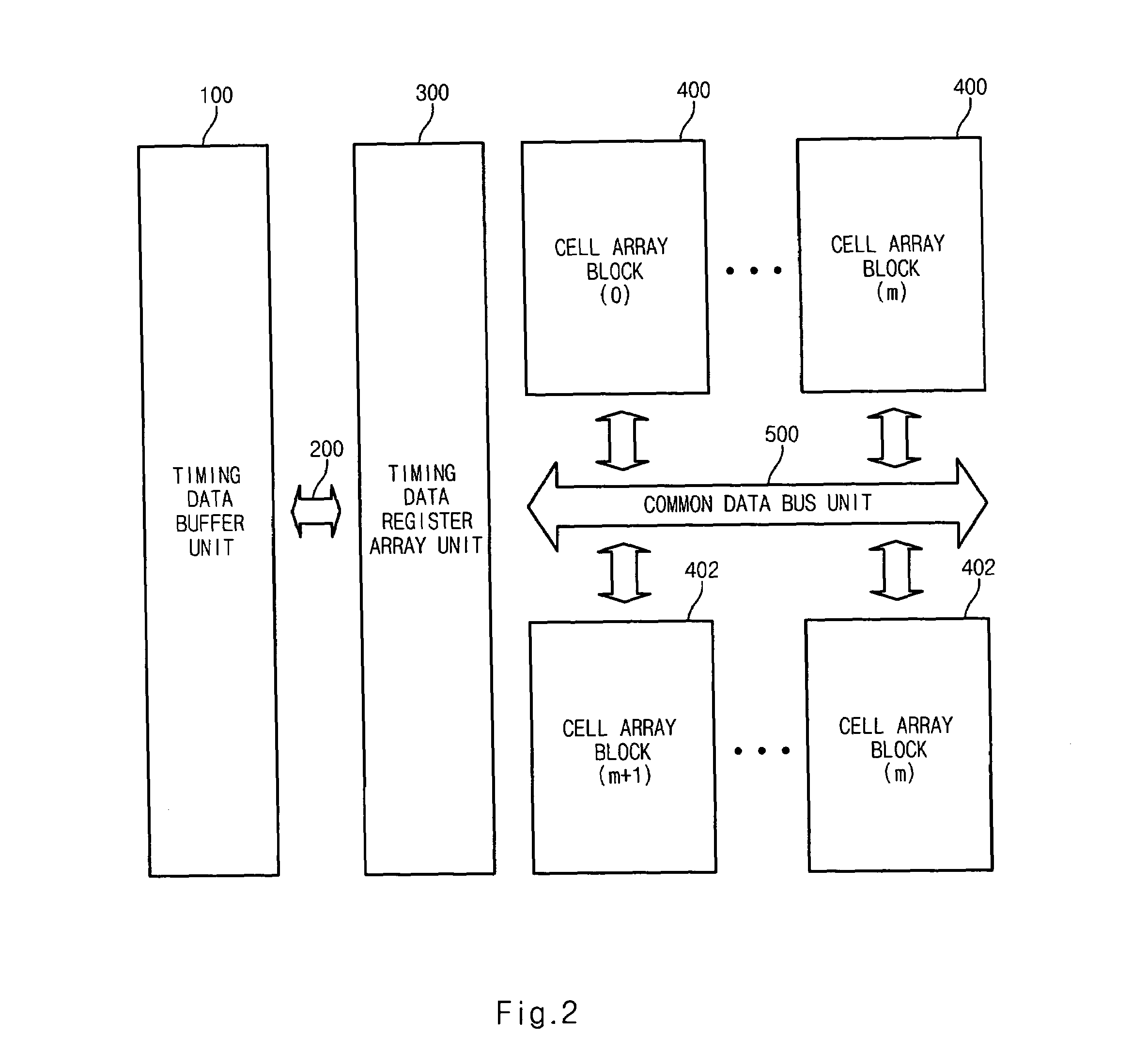
[0045]FIG. 2 is a diagram of a nonvolatile ferroelectric memory device having a multi-bit control function according to the present invention.

[0046]In an embodiment of FIG. 2, a plurality of cell array blocks 400 are arranged above the common data bus unit 500, and a plurality of cell array blocks 402 are arranged under the common data bus unit 500. The common data bus unit 500 is shared by the plurality of cell array blocks 400 and 402. The rest structure is the same as that of FIG. 1.

[0047]FIG. 3 is a diagram of the cell array block 400 of FIGS. 1 and 2.

[0048]The cell array block 400 comprises a MBL (main bitline) pull-up controller 410, a main bitline sensing load unit 420, a plurality of sub cell arrays 430 and a column selecting switch unit 440.

[0049]Here, a main bitline of the plurality of sub cell arrays 430 is connected to the common data bus unit 500 through the column selecting switch unit 440.

[0050]FIG. 4 is a circuit diagram of the main bitline pull-up controller 410 and...


PUM


Abstract

A nonvolatile ferroelectric memory device having a multi control function can determine a plurality of cell data in a reference timing strobe interval by setting a plurality of sensing voltage levels when cell data are sensed in a sensing critical voltage. In a read mode, a plurality of read data applied from a cell array block are stored in a timing data register array unit through a common data bus unit. In a write mode, a plurality of read data stored in the timing data register array unit or input data applied from a timing data buffer unit are stored in a cell array block through the common data bus unit. Here, since a plurality of sensing voltage levels are set in cell data, a plurality of sensed data bits can be stored in one cell.

Description

BACKGROUND OF THE INVENTION[0001]1. Field of the Invention[0002]The present invention generally relates to a nonvolatile ferroelectric memory device having a multi-bit control function, and more specifically, to a technology for storing and sensing multi-bit data in a ferroelectric memory cell.[0003]2. Description of the Prior Art[0004]Generally, a ferroelectric random access memory (hereinafter, referred to as ‘FRAM’) has attracted considerable attention as next generation memory device because it has a data processing speed as fast as a Dynamic Random Access Memory DRAM and conserves data even after the power is turned off.[0005]The FRAM having structures similar to the DRAM includes the capacitors made of a ferroelectric substance, so that it utilizes the characteristic of a high residual polarization of the ferroelectric substance in which data is not deleted even after an electric field is eliminated.[0006]The technical contents on the above FRAM are disclosed in the Korean Pat...

Claims


Application Information

Patent Timeline
Patent Type & Authority Patents(United States)
IPC IPC(8): G11C7/14G11C11/22
CPCG11C11/22
Inventor KANG, HEE BOK
Owner SK HYNIX INC
Why Eureka
Try Eureka