Method for designing semiconductor integrated circuit

a technology of integrated circuits and integrated circuits, applied in the direction of cad circuit design, computer aided design, instruments, etc., can solve the problems of ir drop, slow cell operation, timing change, etc., and achieve the effect of reducing the effect of ir drop, reducing the effective area needed, and reducing processing tim

Inactive Publication Date: 2006-01-17
SOCIONEXT INC
View PDF13 Cites 17 Cited by
  • Summary
  • Abstract
  • Description
  • Claims
  • Application Information

AI Technical Summary

Benefits of technology

[0020]With the foregoing in mind, it is an object of the present invention to provide a method for designing a semiconductor integrated circuit capable of a timing simulation that is approximate to an actual operation by reducing the effect of IR drop on the timing or the amount of IR drop itself without reducing an effective area necessary for arrangement of elements and the number of pads that can be used other than power supply pads and without increasing the processing time.

Problems solved by technology

This is because, in the synchronous design, all flip-flops operate simultaneously in synchronization with a clock signal, and a large amount of electric current flows into a power supply wiring for providing these flip-flops with an electric power, thus causing an IR drop.
When an IR drop occurs, since an amount of power supplied to cells constituting an LSI is reduced, the operations of the cells become slow and thus a timing change occurs.
Therefore, when the timing change occurs due to this IR drop, a timing error may occur in an LSI when it is used as an actual product although it had no timing problem at the verification stage.
The above-mentioned conventional designing methods have such problems as mentioned below.
Firstly, in the design of the power supply wiring in which the number of the power supply wirings or power supply pads are increased so as to suppress the amount of IR drop, there are problems that: it is necessary to increase the number of the power supply wirings, thus reducing the effective area necessary for arrangement of elements; or the number of power supply pads is increased, thus reducing the number of pads that can be used for other than the power supply pads.
Furthermore, in the designing method shown in FIG. 13 in which the IR drop is analyzed and the delay is calculated with the amount of IR drop, at the time of producing the delay library 1302 considering IR drop, characterization at possible various power supply voltages is required for all cells and thus the time for producing the delay library becomes enormous.
Furthermore, in the designing method shown in FIG. 14 in which the layout is generated after the amount of IR drop is predetermined, it is difficult to have all cells operate with the same amount of IR drop.

Method used


Image

  • Method for designing semiconductor integrated circuit
  • Method for designing semiconductor integrated circuit
  • Method for designing semiconductor integrated circuit

Examples


first embodiment

(First Embodiment)

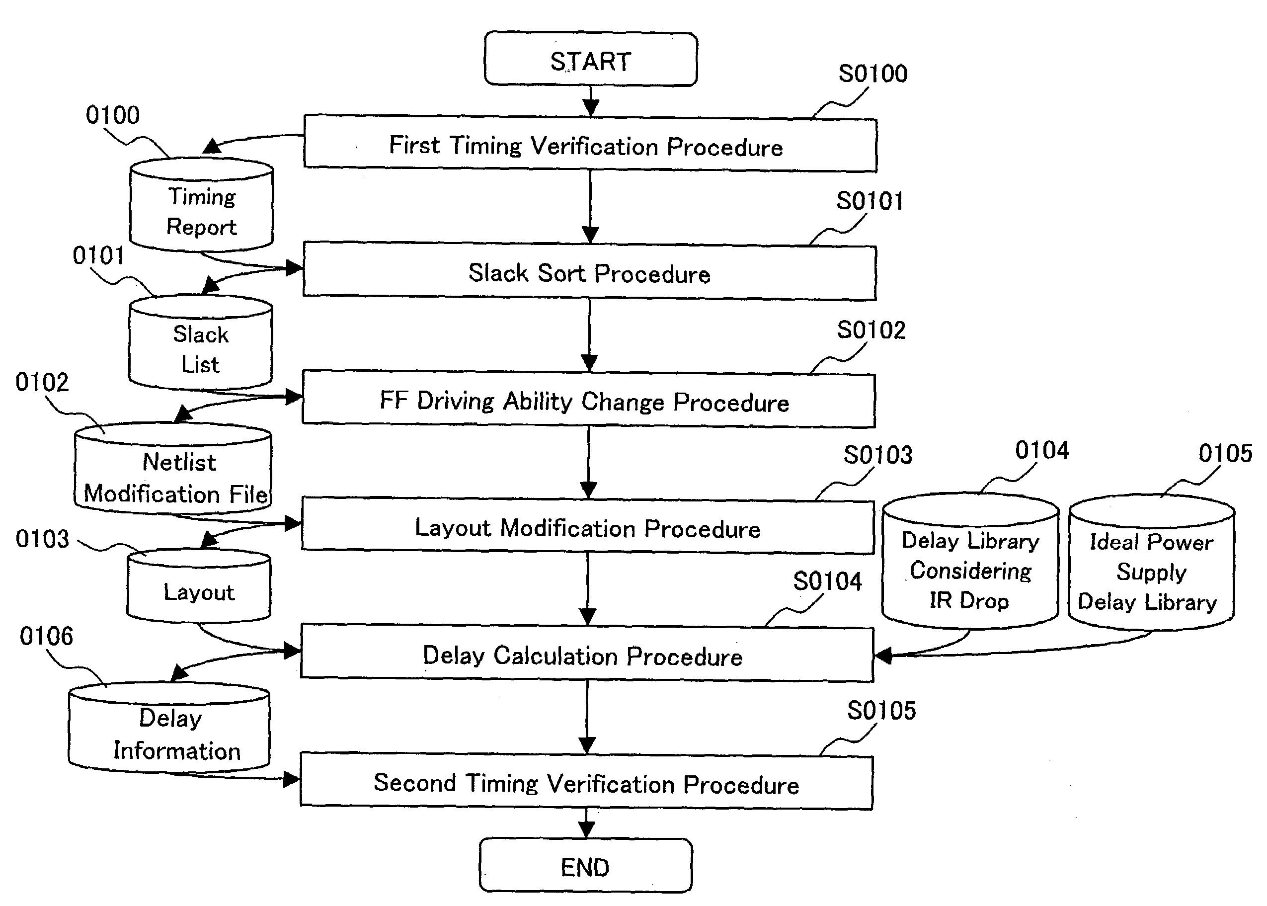
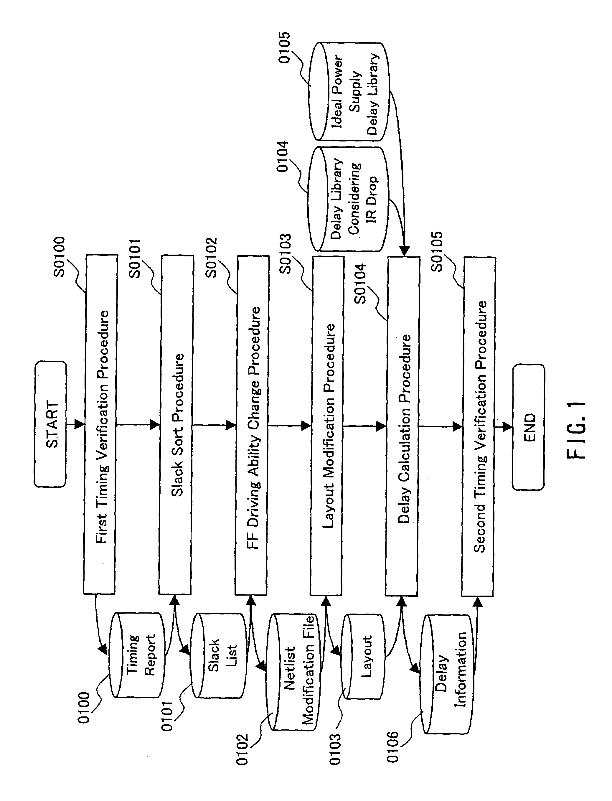
[0049]FIG. 1 is a flowchart showing a method for designing a semiconductor integrated circuit according to a first embodiment of the present invention. In FIG. 1, firstly, in a first timing verification procedure S0100, a netlist, delay information and restriction are input, the timing is verified, and a timing report 0100 of all the paths between flip-flops is output. Herein, the netlist is, for example, a verilog netlist, the delay information is an SDF (Standard Delay Format) and the restriction is a timing restriction file describing the definition of a clock, the designation of a false path and a multicycle path, etc. Furthermore, in the output timing report 0100, a delay time of each cell, a wiring delay time and a slack from a flip-flop at the starting point to a flip-flop at the ending point are described. This timing report 0100 may be such information as can be output easily by any commercial static timing verification tools.

[0050]For example, as shown in...

second embodiment

(Second Embodiment)

[0072]FIG. 5 is a flowchart showing a method for designing a semiconductor integrated circuit according to a second embodiment of the present invention. Note here that in FIG. 5, the same numbers are given to the same parts as those in the configuration of the first embodiment shown in FIG. 1.

[0073]The second embodiment is different from the first embodiment in that a slack sort procedure S0500, a positive / negative FF change procedure S0501 for changing a flip-flop operating at the rising edge of the clock signal into the flip-flop operating at the trailing edge thereof, a slack list 0500, a netlist modification file 0501 and a delay library S0502 considering IR drop are substituted respectively for the slack sort procedure S0101, the FF driving ability change procedure S0102, the slack list 0101, the netlist modification file 0102 and the delay library 0104 considering IR drop. Also, the ideal power supply delay library 0105 is deleted.

[0074]In FIG. 5, in the sla...

third embodiment

(Third Embodiment)

[0086]FIG. 8 is a flowchart showing a method for designing a semiconductor integrated circuit according to a third embodiment of the present invention. Note here that in FIG. 8, the same numbers are given to the same parts as those in the configuration of the first embodiment shown in FIG. 1.

[0087]The third embodiment is different from the first embodiment in that a slack sort procedure S0801, a FF substitution procedure S0801 substituting a buffer for a flip-flop, a slack list 0800, a netlist modification file 0801 and a delay library 0502 considering IR drop are substituted respectively for the slack sort procedure S0101, the FF driving ability change procedure S0102, the slack list 0101 and the netlist modification file 0102. Also, the delay library 0104 considering IR drop and the ideal power supply delay library 0105 are deleted and an additional timing restriction 0802 is added as a result of substituting the buffer for the flip-flop.

[0088]In FIG. 8, in the s...


PUM


Abstract

A method for designing a semiconductor integrated circuit is provided that is capable of a timing simulation that is approximate to an actual operation by reducing the effect of IR drop on the timing without reducing an effective area necessary for arrangement of elements or the number of pads that can be used other than power supply pads and without increasing the processing time. In a FF driving ability change procedure, a flip-flop having a delay time larger than a transition time from a state in which an IR drop occurs in a power supply voltage to a state of an ideal power supply voltage is substituted for an arbitrary flip-flop. Thus, a delay library considering IR drop may be produced previously only for the flop-flop, thus enabling a production time of the library to be reduced and improving the calculation accuracy of the delay time in the delay calculation procedure. Furthermore, the substitution of a flip-flop having a low driving ability enables the area to be reduced.

Description

BACKGROUND OF THE INVENTION[0001]1. Field of the Invention[0002]The present invention relates to a method for designing a semiconductor integrated circuit. In particular, it relates to a technology for controlling a timing with respect to a voltage drop (referred to as an IR drop hereinafter) caused by a resistance component of a power supply wiring in a semiconductor integrated circuit, and a method for designing a circuit in which the effect of an IR drop is reduced.[0003]2. Description of the Related Art[0004]Recently, as the size of LSI has been increased and lower electric power has been demanded, various kinds of physical phenomena have become significant. Therefore, unless such physical phenomena are taken into consideration at the designing stage, a phenomenon occurs in which a semiconductor integrated circuit operates in simulation but does not operate as an actual product. In particular, a phenomenon referred to as an IR drop, caused by a resistance component of a power su...

Claims


Application Information

Patent Timeline
Patent Type & Authority Patents(United States)
IPC IPC(8): G06F17/50H01L21/82
CPCG06F17/5045G06F17/5031G06F30/3312G06F30/30G06F30/3315G06F2119/12
Inventor IWANISHI, NOBUFUSASATOH, KAZUHIROISHIBASHI, NORIKO
Owner SOCIONEXT INC
Why Eureka
Try Eureka