Method for preventing to form a spacer undercut in SEG pre-clean process

a technology of spacers and pre-cleaning, applied in the direction of basic electric elements, electrical apparatus, semiconductor devices, etc., can solve the problems of leakage current between sources, drains and gates, etc., and achieve the effect of preventing leakage curren

Inactive Publication Date: 2006-01-31
MARLIN SEMICON LTD
View PDF13 Cites 68 Cited by
  • Summary
  • Abstract
  • Description
  • Claims
  • Application Information

AI Technical Summary

Benefits of technology

[0008]In accordance with the present invention, a method for providing an improved etching process which utilizes a HFEG (HF diluted by ethylene glycol) solution to etch oxide and nitride simultaneously. Compare to oxide, nitride is etched comparatively faster than oxide is. It is an objective of the present invention to provide a method for improvement in formation of an undercut in Pre-clean process that utilizes a hydrofluoric acid solution to remove the native oxide on the semiconductor substrate in the prior art. It is another objective of the present invention is that provides a method for obtaining a clean surface of the semiconductor in order to form raised source and drain structure with SEG technique. It is yet another objective of the present invention is that provides a method for preventing leakage current is formed between raised source / drain and gate because of formation of the spacer undercut in Pre-clean process.

Problems solved by technology

However, employing hydrofluoric acid in order to remove the oxide on the silicon substrate that will produce a spacer undercut and result in leakage current between source, drain and gate.
Due to the fact that utilizes a hydrofluoric acid solution in order to remove the native oxide, a spacer undercut is created and result in leakage current between source, drain and gate.

Method used


Image

  • Method for preventing to form a spacer undercut in SEG pre-clean process
  • Method for preventing to form a spacer undercut in SEG pre-clean process
  • Method for preventing to form a spacer undercut in SEG pre-clean process

Examples


Embodiment Construction

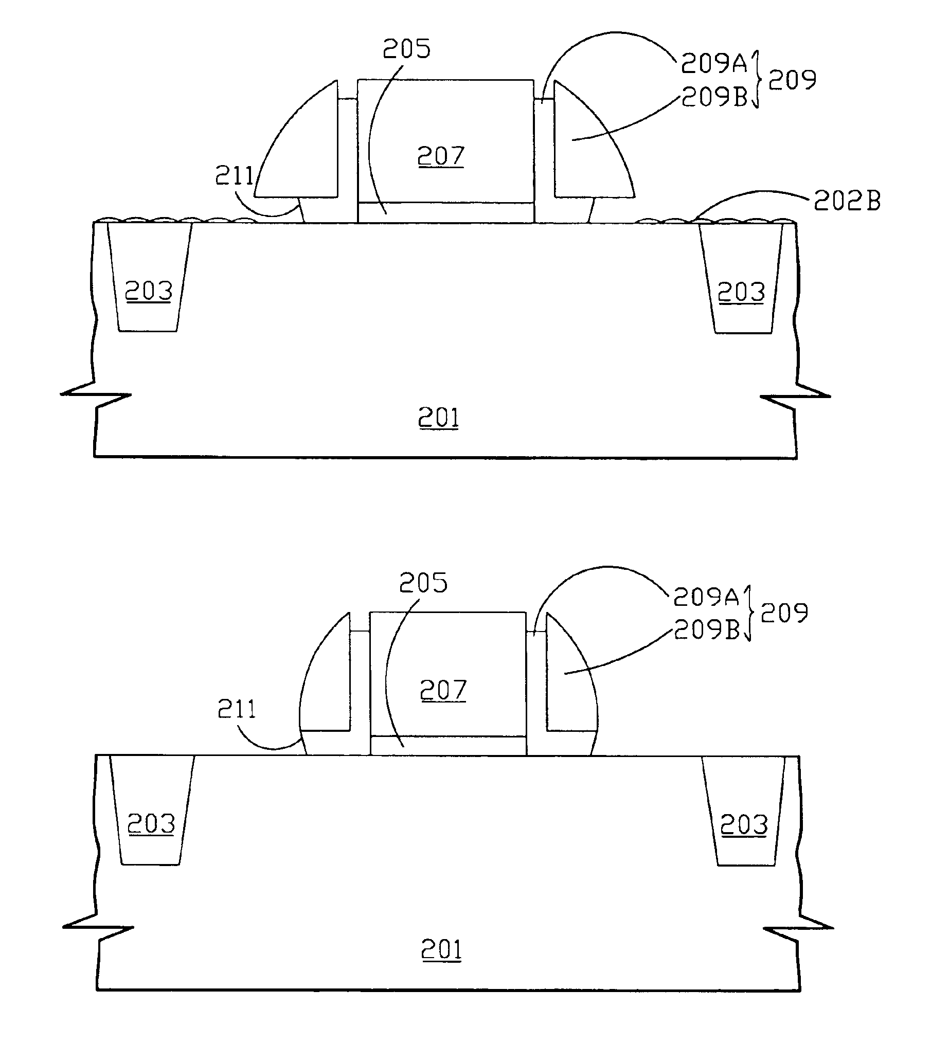
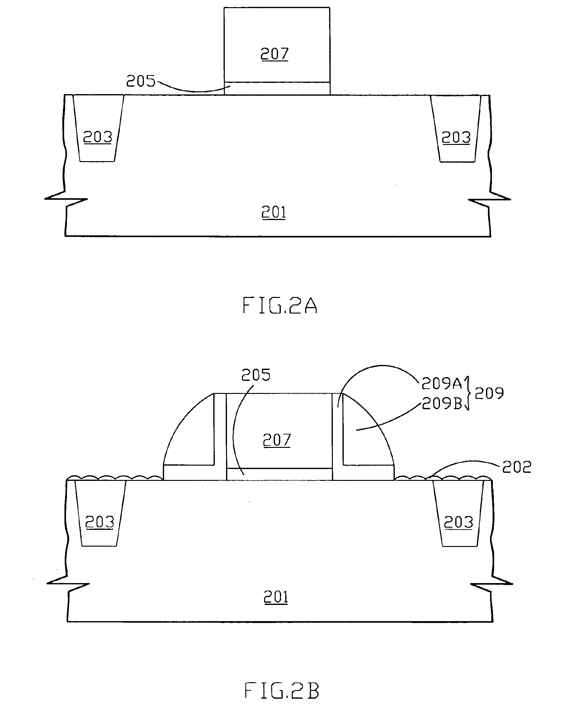
[0014]Preferred embodiment of this invention will be explained with reference to the drawings of FIGS. 2A to 2E. Referring to FIG. 2A, a semiconductor substrate 201 is provided firstly; for instance silicon dioxide. An oxide layer (not illustrated) is deposited on the semiconductor substrate 201; for instance silicon dioxide. A dielectric layer (not illustrated) is deposited on the oxide layer; for instance silicon nitride. The oxide and nitride layers are defined as a mask layer of an active region in the semiconductor substrate 201. Thereafter, etching a portion of the mask layers through a dry etching process, and dry etching is performed and stopped within the semiconductor substrate 201 so as to form a plurality of shallow trench. Then, the surfaces of shallow trench have an oxidation so that the damage on the shallow trench surface will be filled and repaired. Subsequently, performing trench filling with silicon dioxide by chemical vapor deposition (CVD) technique and planariz...


PUM


Abstract

A method for preventing to form a spacer undercut in SEG preclean process is provided. This present invention utilizes HFEG solution to etch the first spacer and the second spacer simultaneously, which can prevent from producing a spacer undercut, meanwhile; a native oxide layer upon a surface of a semiconductor substrate is removed. Hence, the clean surface on the semiconductor substrate is obtained. This method includes the steps as follows: Firstly, the native oxide layer upon the surface of the semiconductor substrate is removed by DHF (HF in deionized water) solution. Then, etching the first spacer and the second spacer at the same time by HFEG (HF diluted by ethylene glycol) solution. Also, the native oxide upon the semiconductor substrate is removed. Therefore, it obtains the clean semiconductor surface without a serious spacer undercut.

Description

BACKGROUND OF THE INVENTION[0001]1. Field of the Invention[0002]The present invention relates to a method of preventing to form a spacer undercut, and more particularly to a method of etching the oxide and nitride spacer simultaneously to prevent from forming a spacer undercut in SEG Pre-clean process.[0003]2. Description of the Prior Art[0004]Generally, as semiconductor dimensions continue to shrink and device densities increase, contact resistance and junction depth become increasingly critical for device performance. Raised source and drain structures can provide shallow junctions with low series resistance, enhancing performance. Raised source and drain structures are typically fabricated using selective epitaxial growth (SEG) method which need a clean surface of silicon substrate; however, the surface of silicon substrate is accessible to form a native oxide with aqueous and oxygen atom from the air, for instance a silicon dioxide layer. Therefore, it is generally utilized hydr...

Claims


Application Information

Patent Timeline
Patent Type & Authority Patents(United States)
IPC IPC(8): H01L21/336H01L21/302H01L21/306H01L21/311H01L21/461H01L29/78
CPCH01L21/02052H01L21/31111H01L29/7834H01L29/6656H01L29/66628H01L29/6653
Inventor CHENG, YA-LUNCHIEN, CHIN-CHENGYANG, NENG-HUICHEN, YU-KUN
Owner MARLIN SEMICON LTD
Why Eureka
Try Eureka