Method of producing a semiconductor structure having at least one support substrate and an ultrathin layer

a technology of support substrate and semiconductor structure, which is applied in the direction of semiconductor devices, electrical equipment, basic electric elements, etc., can solve the problems of thin layer not being able to withstand subsequent heat treatment, defects, and appearance of defects, and achieve the effect of reducing thickness

Active Publication Date: 2006-01-31
S O I TEC SILICON ON INSULATOR THECHNOLOGIES +1
View PDF8 Cites 56 Cited by
  • Summary
  • Abstract
  • Description
  • Claims
  • Application Information

AI Technical Summary

Benefits of technology

[0012]Presented is a method of producing a semiconductor structure having at least one support substrate and an ultrathin layer. The method includes bonding a support substrate to a source substrate, detaching a useful layer along a zone of weakness to obtain an intermediate structure including at least the transferred useful layer and the support substrate, and treating the transferred useful layer to obtain an ultrathin layer on the su

Problems solved by technology

However, experiments have shown that when the thin layer to be transferred is very thin, meaning less than about 100 nanometers (nm), defects appear which do not occur when transferring a thicker layer.
Such a very thin layer will not withstand subsequent heat treatments conducted either to strengthen its bonding interface with the support substrate, or to detach it from the source substrate.
The heat treatments increase the pressure that exists in gas microbubbles present in the zone of weakness and cause them to degas, resulting in the formation of defects.
Similarly, when an intermediate layer is present between the thin layer to be transferred and the support substrate, it has been shown that the thinner the transferred thin layer, the more d

Method used


Image

  • Method of producing a semiconductor structure having at least one support substrate and an ultrathin layer
  • Method of producing a semiconductor structure having at least one support substrate and an ultrathin layer
  • Method of producing a semiconductor structure having at least one support substrate and an ultrathin layer

Examples


example 1

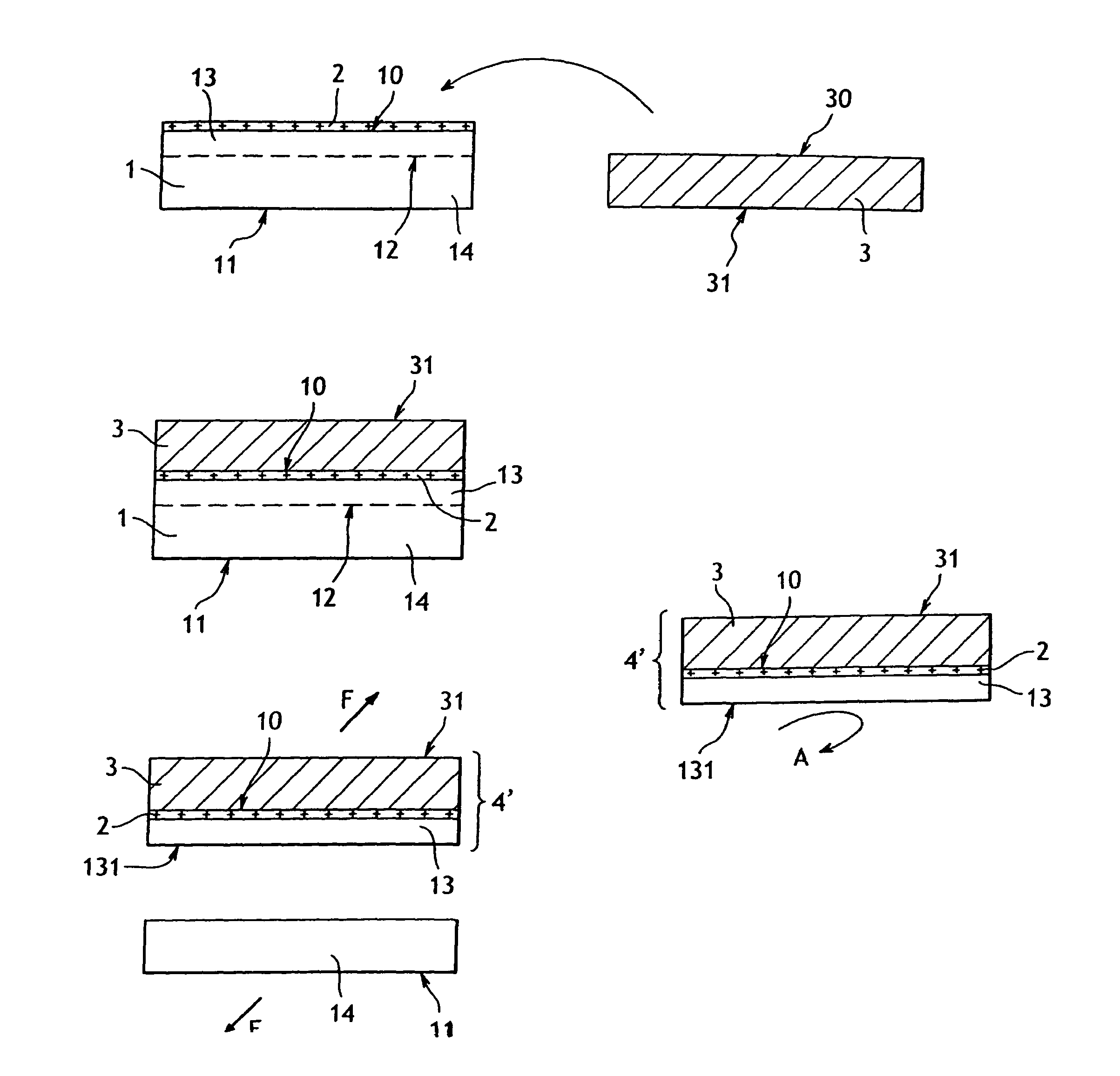
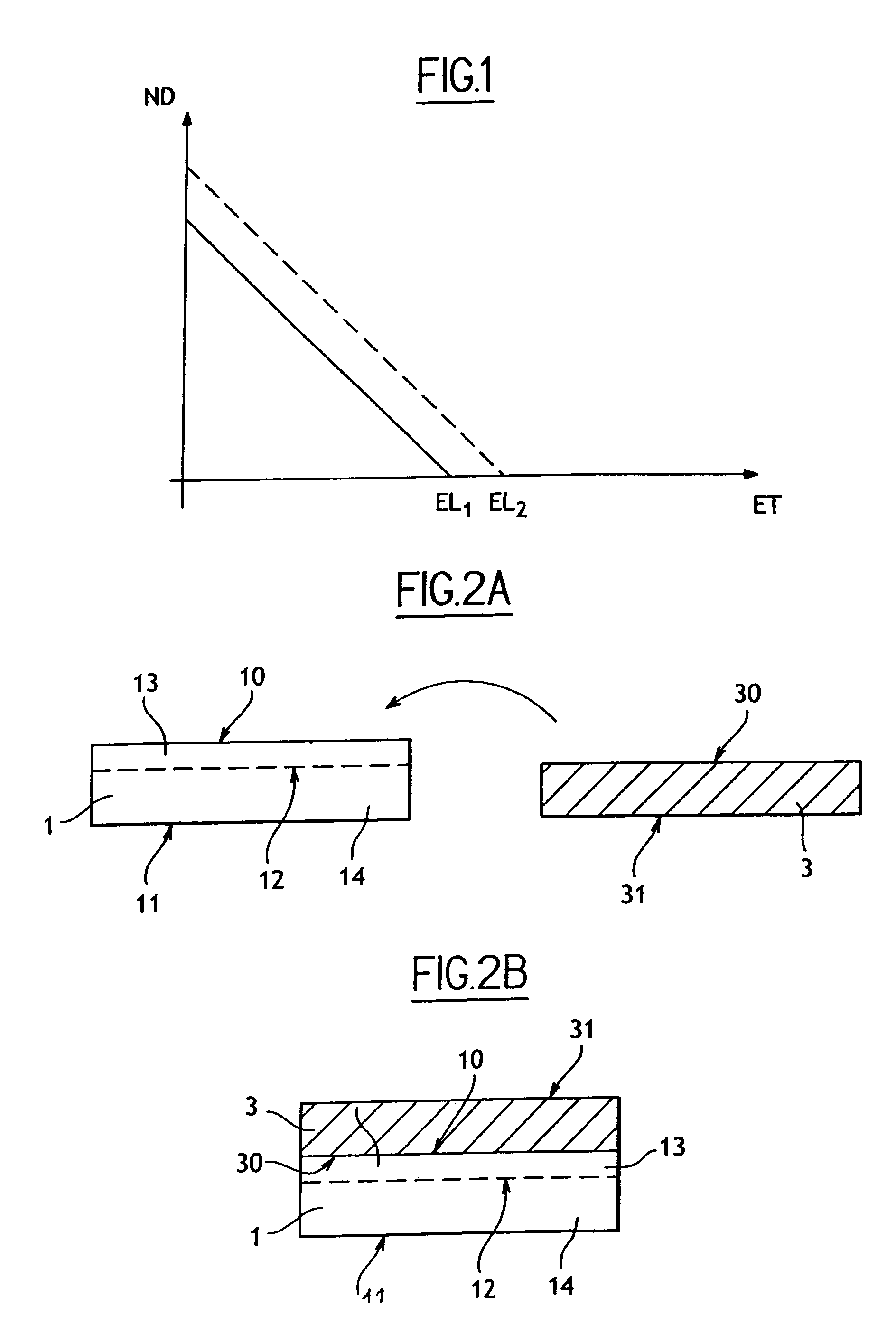
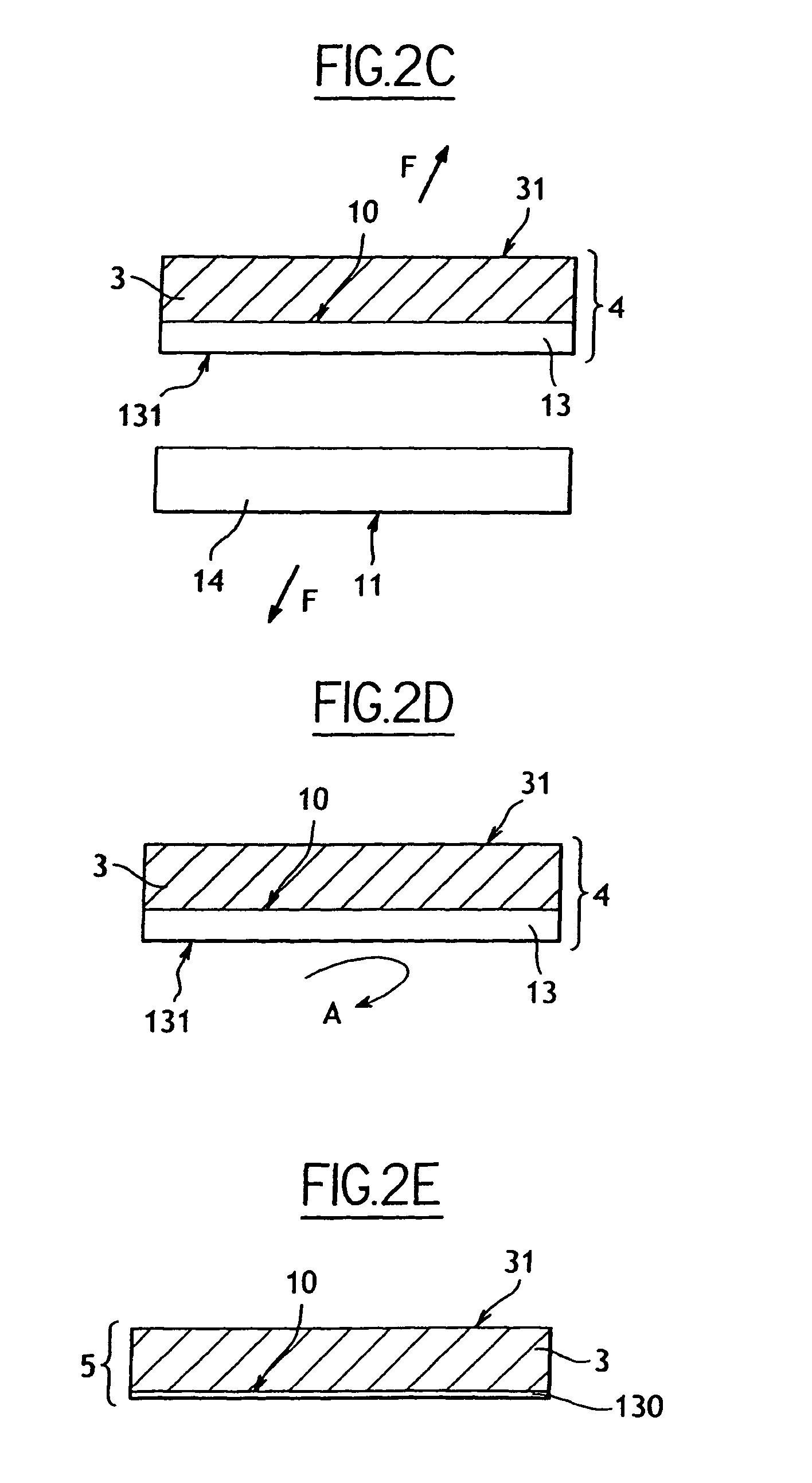
[0048]Thermal oxidation of a source substrate 1 formed from bulk silicon was carried out to cover it with an intermediate layer 2 of silicon oxide (SiO2) that was about 50 nanometers thick. The zone of weakness 12 was then formed by implanting hydrogen ions H+ using an implantation dose of 8×10¹⁶H+ / cm2 and an implantation energy of 210 keV to obtain a useful layer 13 with a thickness of about 1.9 micrometers (1.9 μm). The bulk silicon support substrate was then bonded to the oxide layer 2 by wafer bonding. The remainder 14 of the source substrate 1 was then detached by using a heat treatment of less than 500° C., and the bonding interface was strengthened by using a heat treatment of more than about 1000° C. Finally, a thinning treatment was conducted using polishing and sacrificial oxidation to obtain a final structure 5′ with an ultrathin silicon layer 130 having a thickness of about 50 nm, which could have been reduced further to 20 nm thick if the thinning step was continued.

example 2

[0049]The procedure described above concerning Example 1 was followed, except that the silicon oxide layer 2 was 20 nanometers thick.

example 3

[0050]The procedure described above concerning Example 1 was followed, except that the implantation dose was 7×10¹⁶H+ / cm2 and the implantation energy was 160 keV, so that the useful layer 13 was 1.5 micrometers (1.5 μm) thick.


PUM


Abstract

A method of producing a semiconductor structure having at least one support substrate and an ultrathin layer. The method includes bonding a support substrate to a source substrate, detaching a useful layer along a zone of weakness to obtain an intermediate structure including at least the transferred useful layer and the support substrate, and treating the transferred useful layer to obtain an ultrathin layer on the support substrate. The source substrate includes a front face and a zone of weakness below the front face that defines the useful layer, and the useful layer is sufficiently thick to withstand heat treatments without forming defects therein so that it can be reduced in thickness to form the ultrathin layer. The resulting ultrathin layer is suitable for use in applications in the fields of electronics, optoelectronics or optics.

Description

BACKGROUND ART[0001]The present invention generally relates to a method of producing a structure including at least one support substrate and an ultrathin layer of a semiconductor material. An embodiment of the invention advantageously includes an intermediate layer between the support substrate and the ultrathin layer.[0002]Composite substrates are fabricated for use in the fields of optics, electronics, or optoelectronics. During fabrication, layer transfer methods can be used to transfer a layer from a source substrate onto a support substrate. One such layer transfer method includes implanting atomic species beneath the surface of a source substrate to create a zone of weakness therein which defines a thin layer. The free face of the thin layer is then brought into intimate contact or bonded with the support substrate. The thin layer is then detached from the remainder of the source substrate to transfer it to the support substrate. This type of method is known as the “SMART-CUT...

Claims


Application Information

Patent Timeline
IPC IPC(8): H01L21/30H01L21/46H01L21/762
CPCH01L21/76259H01L21/76254H01L27/12
Inventor AULNETTE, CECILEBATAILLOU, BENO TGHYSELEN, BRUNOMORICEAU, HUBERT
Owner S O I TEC SILICON ON INSULATOR THECHNOLOGIES
Why Eureka
Try Eureka