Gallium arsenide antimonide (GaAsSB)/indium phosphide (InP) heterojunction bipolar transistor (HBT) having reduced tunneling probability

a bipolar transistor and heterojunction technology, applied in the field ofgallium arsenide antimonide (gaassb)/indium phosphide (inp) heterojunction bipolar transistor (hbt) having reduced tunneling probability, can solve the problem of insufficient breakdown voltage for a number of potential applications, and achieve the effect of increasing the breakdown voltage of an hbt and reducing the probability of electron tunneling

Inactive Publication Date: 2006-01-31
AGILENT TECH INC
View PDF11 Cites 4 Cited by
  • Summary
  • Abstract
  • Description
  • Claims
  • Application Information

AI Technical Summary

Benefits of technology

[0007]The tunneling suppression layer increases the breakdown voltage of an HBT by decreasing the probability of electrons tunneling from the valence band of the base to the conduction band of the collector.

Problems solved by technology

GaAsSb / InP HBTs have the above-described advantages but also a breakdown voltage insufficient for a number of potential applications.

Method used


Image

  • Gallium arsenide antimonide (GaAsSB)/indium phosphide (InP) heterojunction bipolar transistor (HBT) having reduced tunneling probability
  • Gallium arsenide antimonide (GaAsSB)/indium phosphide (InP) heterojunction bipolar transistor (HBT) having reduced tunneling probability
  • Gallium arsenide antimonide (GaAsSB)/indium phosphide (InP) heterojunction bipolar transistor (HBT) having reduced tunneling probability

Examples


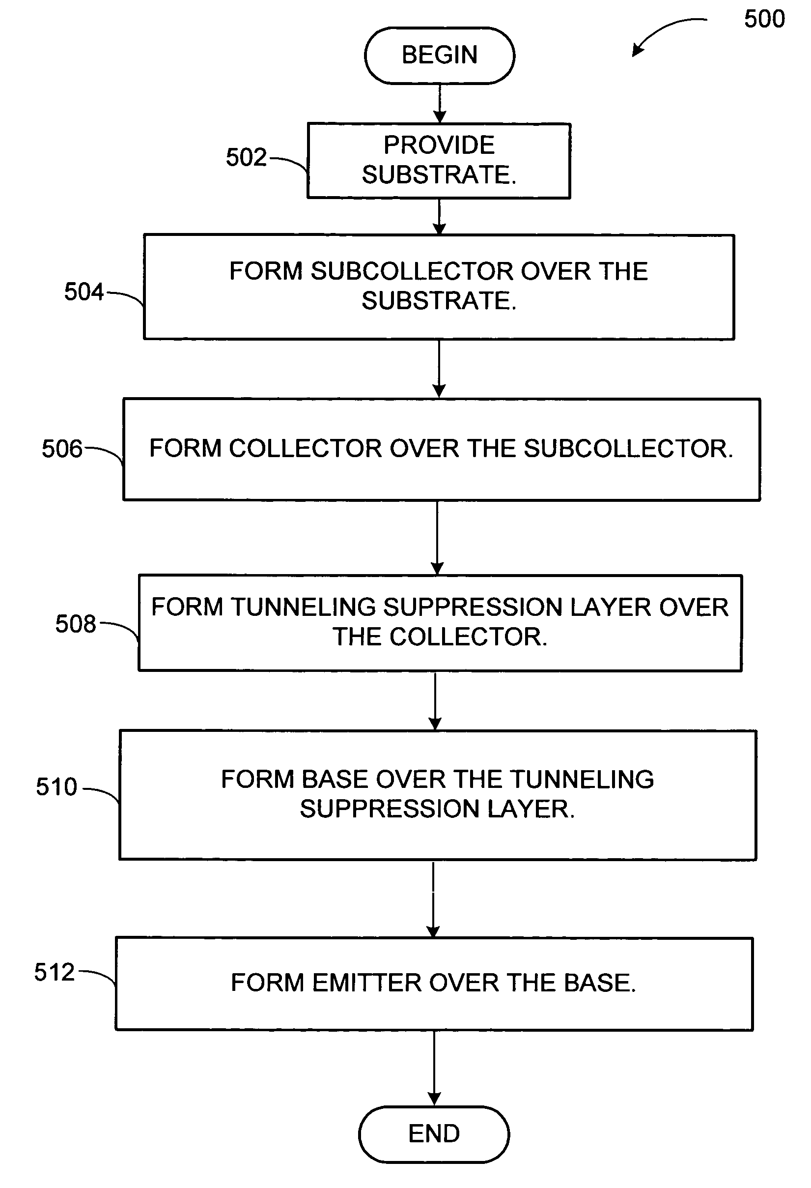
Embodiment Construction

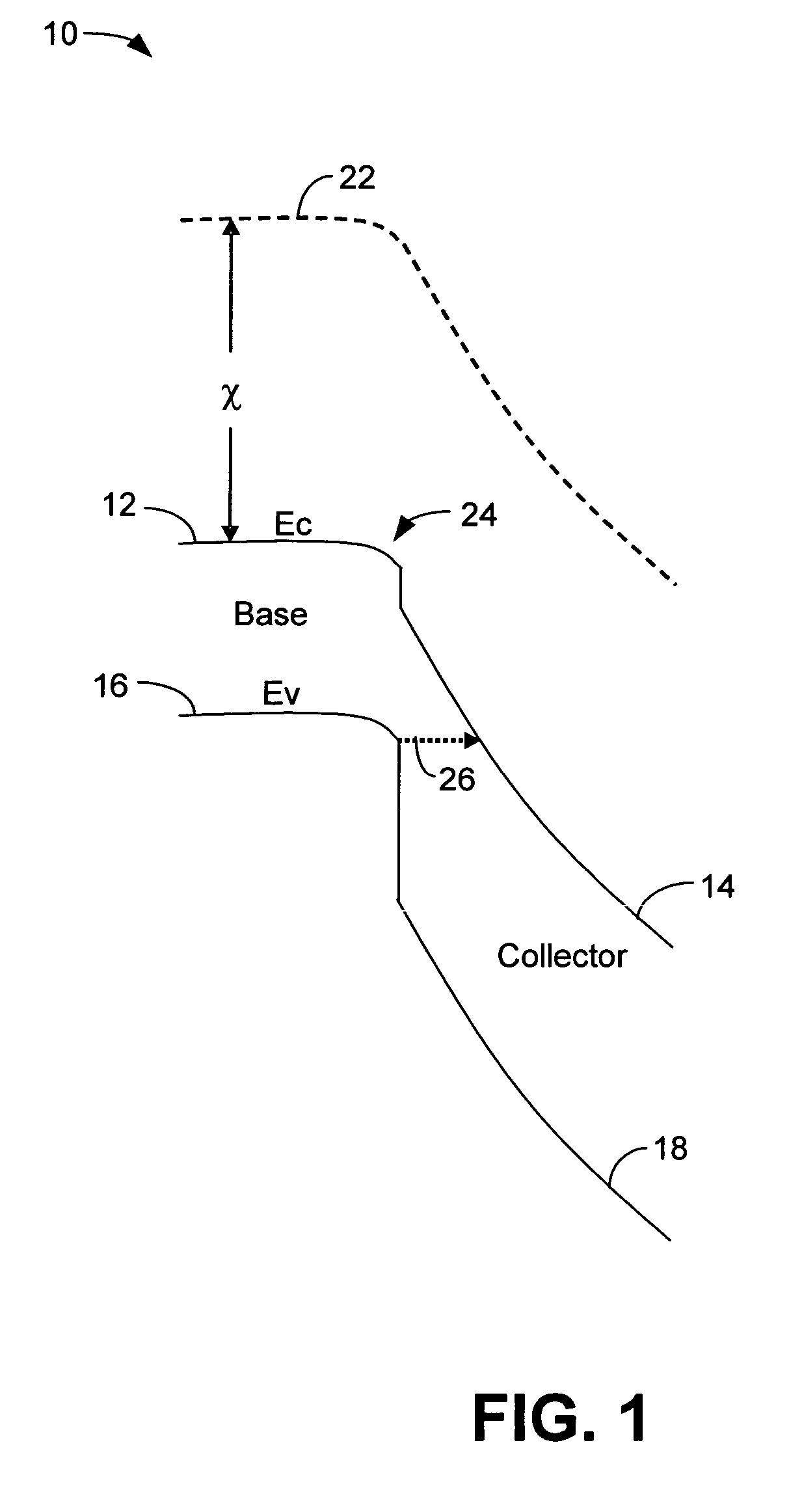
[0017]A band diagram 10 for the base-collector junction of an HBT having a GaAsSb base and an InP collector is shown in FIG. 1 and shows a type-II band lineup. The band diagram 10 plots electron energy against physical distance in the direction orthogonal to the plane of the layers of the device. The band diagram 10 shows the conduction band energy, Ec, (12 for the base and 14 for the collector) the valence band energy Ev, (16 for the base and 18 for the collector) and the vacuum level 22 under reverse bias. The vacuum level is a reference defining the energy of a free electron. The electron affinity, χ (chi), is the difference in energy between the vacuum level 22 and the conduction band energy, Ec, of a semiconductor. The electron affinity, χ, is the energy needed to free an electron present in the conduction band of a semiconductor. Since the vacuum level is continuous, the conduction band offset is the difference in the electron affinity between two semiconductors.

[0018]The band...


PUM


Abstract

A heterojunction bipolar transistor (HBT), comprises a collector formed over a substrate, a base formed over the collector, an emitter formed over the base, and a tunneling suppression layer between the collector and the base, the tunneling suppression layer fabricated from a material that is different from a material of the base and that has an electron affinity equal to or greater than an electron affinity of the material of the base.

Description

BACKGROUND OF THE INVENTION[0001]An indium phosphide (InP)-based heterojunction bipolar transistor (HBT) is useful in applications where high-frequency operation and relatively high breakdown voltage, on the order of 10 to 20 volts, is desirable. The approximate relationship fMAX=√{square root over (fT / 8πRbCc)}, where fT is the current-gain-bandwidth product, or cutoff frequency, Rb is the base series resistance and Cc is the collector-base capacitance, shows that as fT increases, the maximum operating frequency fMAX increases. The relationship is approximate because it is based on a simple lumped-element model of the transistor. Actually, the base series resistance Rb and collector-base capacitance Cc are distributed. More accurate expressions are algebraically complex and would obscure, rather than illuminate, the points that this approximate expression is used to make.[0002]The breakdown voltage of a p-n junction is the reverse voltage beyond which a small increase in voltage cau...

Claims


Application Information

Patent Timeline
Patent Type & Authority Patents(United States)
IPC IPC(8): H01L31/0328H01L21/331H01L29/08H01L29/737
CPCH01L29/0821H01L29/7371H01L29/66318
Inventor BAHL, SANDEEPMOLL, NICOLAS J.
Owner AGILENT TECH INC
Why Eureka
Try Eureka