Method of manufacturing a semiconductor device

a manufacturing method and semiconductor technology, applied in the direction of identification means, instruments, optics, etc., can solve the problems of difficult to manufacture thin-film transistors on their surface, low heat resistance of resin substrates, and difficult to improve such characteristics in view of the relationship of substrates as used, etc., to promote silicon crystallization and simple use of solvents

Inactive Publication Date: 2006-02-14
SEMICON ENERGY LAB CO LTD
View PDF57 Cites 176 Cited by
  • Summary
  • Abstract
  • Description
  • Claims
  • Application Information

AI Technical Summary

Benefits of technology

[0052]In the structures described in this specification, one kind or plural kinds of elements selected from Fe, Co, Ni, Ru, Rh, Pd, Os, Ir, Pt, Cu and Au can be used for the metal element that promotes the crystallization of silicon. In particular, Ni can obtain the higher reproducibility and effects.

Problems solved by technology

However, under the existing circumstance, it is difficult to improve such characteristics in view of the relationship of the substrate as used.
Of them, the resin substrate is low in a heat-resistance, and therefore it is hard to manufacture the thin-film transistor on its surface.
Also, the quartz substrate can withstand a high temperature of 1000° C. or more, however, it is expensive and causes an economical problem when the display unit is enlarged.
However, in order to form the crystalline silicon thin film, a sample must be exposed to a high-temperature atmosphere, and in the case of using the glass substrate, there arises such a problem that the substrate is warped or deformed.
In particular, when making the substrate large in area, that problem becomes remarkable.
However, in the SOI technique under the existing circumstance, it is difficult to form a monocrystal thin film in a large area of 10 inch diagonal or more.

Method used


Image

  • Method of manufacturing a semiconductor device
  • Method of manufacturing a semiconductor device
  • Method of manufacturing a semiconductor device

Examples


first embodiment

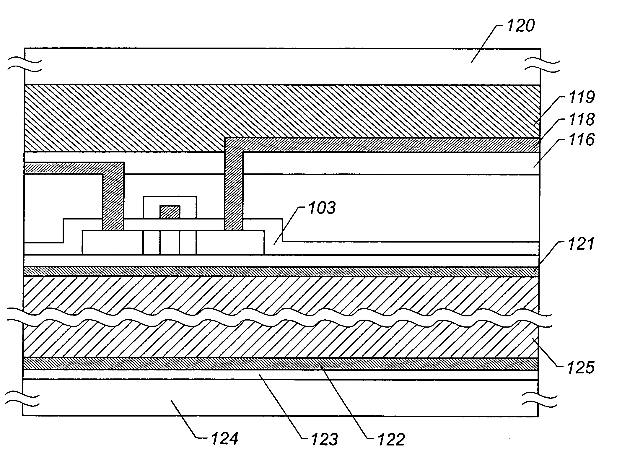
[0100]A first embodiment relates to an example in which a liquid-crystal display thin-film integrated circuit having a large area which has been fabricated on a glass substrate at a low-temperature process of 550° C. or lower is transferred from the glass substrate onto a PET (polyethylene terephthalate) which is of a flexible substrate to constitute an active matrix liquid-crystal display unit which can be disposed even on a curved surface. More particularly, in this embodiment, the structure of a pixel region will be described. In this description, a liquid-crystal display unit is shown as one example, however, a technique described in this specification is available to the EL-type display unit.

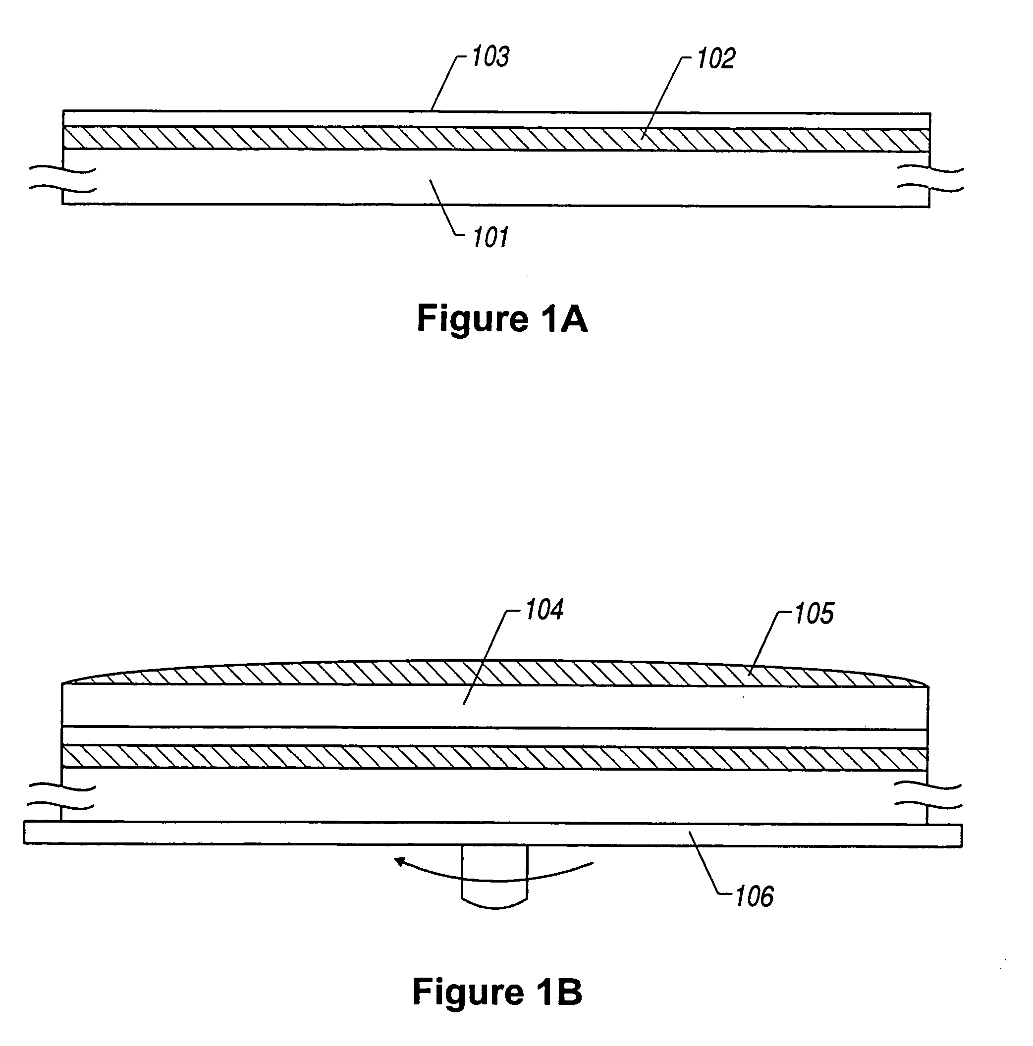
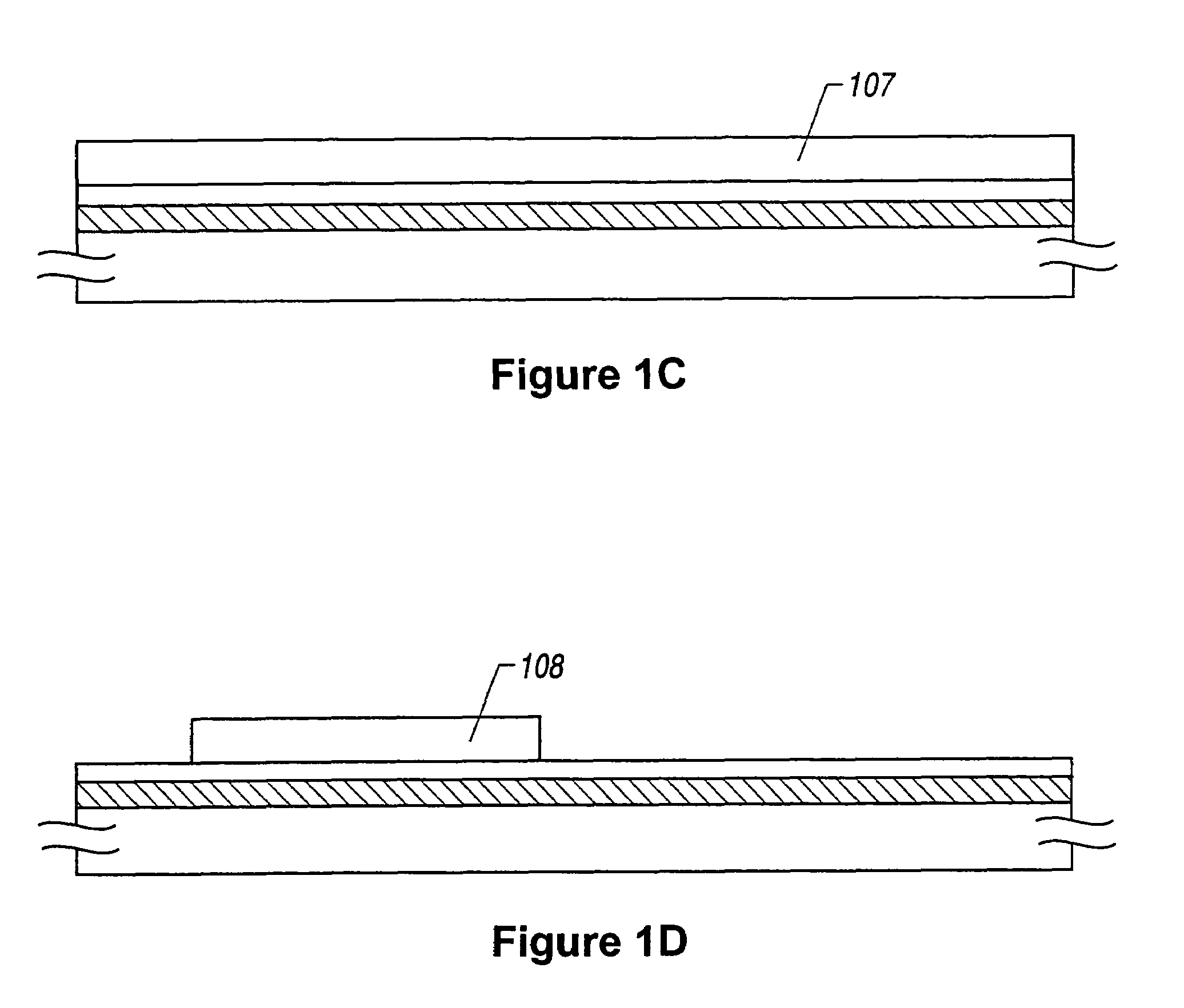
[0101]First, a glass substrate 101 is prepared. Fine concave portions have been formed on a surface of the glass substrate 101 in advance. In this example, the concave portions are several thousands A to several μm in width and height, several to several tens μm in depth, and shaped in the ...

second embodiment

[0127]A second embodiment is an example in which Cu (copper) is used as a metal element that promotes the crystallization of silicon in the process described with reference to the first embodiment. In this embodiment, copper elements are introduced using copper (II) acetate (Cu(CH3COO)2) solution. The density of the copper elements in that solution is adjusted so that the density of copper elements that remain in a final silicon film is set to 1×10¹⁶ to 5×10¹⁹ atms cm−3.

[0128]In the case of using Cu as the metal element that promotes the crystallization of silicon, a heat treatment for crystallization is conducted under a condition of 580° C. and 4 hours. This is because Cu is slightly small in function that promotes the crystallization of silicon in comparison with Ni. Other structures and process conditions are the same as those shown in the first embodiment.

third embodiment

[0129]A third embodiment shows an example in which a silicon film having a monocrystal-like region or substantially monocrystal-like region is formed on a glass substrate, and the active matrix liquid-crystal display unit having a flexible structure is constituted using this silicon film.

[0130]In this example, a Corning 7059 glass substrate (warp point 593° C.) is used as a glass substrate 501. Lattice-like or stripe-like grooves which are several μm in width and several to several tens μm in depth have been formed in advance.

[0131]First, a peeling layer 502 is formed on a glass substrate 501. The peeling layer 502 is of a silicon oxide film using the above-mentioned OCD solution. In this situation, fine gaps are formed on the bottom portion of the grooves because of the existence of the above-mentioned grooves.

[0132]Then, a silicon oxide film 503 is formed on the peeling layer 502 through the plasma CVD technique using the TEOS gas. Since the silicon oxide film 503 serves as a supp...


PUM

PropertyMeasurementUnit
temperatureaaaaaaaaaa
sizeaaaaaaaaaa
temperatureaaaaaaaaaa

Abstract

A method of manufacturing a semiconductor device, comprises the steps of: forming a first insulating film on a first substrate; forming a second insulating film on the first insulating film; forming an amorphous silicon film on the second insulating film; holding a metal element that promotes the crystallization of silicon in contact with a surface of the amorphous silicon film; crystallizing the amorphous silicon film through a heat treatment to obtain a crystalline silicon film; forming a thin-film transistor using the crystalline silicon film; forming a sealing layer that seals the thin-film transistor; bonding a second substrate having a translucent property to the sealing layer; and removing the first insulating film to peel off the first substrate.

Description

[0001]This is a continuation of U.S. application Ser. No. 08 / 602,324, filed Feb. 16, 1996, now U.S. Pat. No. 5,821,138.BACKGROUND OF THE INVENTION[0002]1. Field of the Invention[0003]The present invention relates to a technique by which a display panel which is flexible (having a flexibility) is provided, and more particularly to a technique by which a flexible active matrix liquid-crystal display unit is provided.[0004]2. Description of the Related Art[0005]There has been known a liquid-crystal display unit as a display unit which is small-sized, light in weight and of the thin type. This has a structure in which liquid crystal is interposed between a pair of translucent substrates which are bonded to each other at intervals of several μm and held in this state as the structure of a display panel. In the operation of the display unit, an electric field is applied to liquid crystal in a predetermined region so as to change its optical characteristics, whereby the presence / absence of...

Claims


Application Information

Patent Timeline
Patent Type & Authority Patents(United States)
IPC IPC(8): H01L21/30H01L21/84G02F1/13A42B3/22G02F1/1333G02F1/136G02F1/1368G09F9/30H01L21/02H01L21/20H01L21/265H01L21/336H01L21/77H01L27/12H01L27/32H01L29/786
CPCH01L21/2022H01L27/1266H01L29/66757H01L27/1277H01L2221/68318H01L2221/68363Y10S438/928Y10S438/977H01L2221/68359H01L21/02422H01L21/02532H01L21/02672H01L21/02675
Inventor YAMAZAKI, SHUNPEIARAI, YASUYUKITERAMOTO, SATOSHI
Owner SEMICON ENERGY LAB CO LTD
Why Eureka
Try Eureka