SOI wafer producing method, and wafer separating jig

a soi wafer and production method technology, applied in the field of soi wafer and wafer separation jig, can solve the problems of reducing the yield ratio, difficult to separate both wafers, scratching on the surface, etc., and achieve the effect of improving the yield ratio

Inactive Publication Date: 2006-02-14
SHIN-ETSU HANDOTAI CO LTD
View PDF12 Cites 15 Cited by
  • Summary
  • Abstract
  • Description
  • Claims
  • Application Information

AI Technical Summary

Benefits of technology

[0016]Use of the wafer separation jig of this invention makes it possible to readily separate, for example, the aforementioned stack comprising the SOI wafer and the residual wafer into the individual wafers without causing scratches on the major surfaces thereof, and to improve the yield ratio in the fabrication more than use of a vacuum chuck.

Problems solved by technology

Use of the vacuum chuck as shown in FIG. 7, however, makes it difficult to separate both wafers while keeping a parallel positional relation so as to avoid contact therebetween.
Any accidental friction between both wafers to be separated may result in scratching on the surface.
The scratching in particular on the SOI wafer is undesirable because it may result in a lowered yield ratio.

Method used


Image

  • SOI wafer producing method, and wafer separating jig
  • SOI wafer producing method, and wafer separating jig
  • SOI wafer producing method, and wafer separating jig

Examples


example

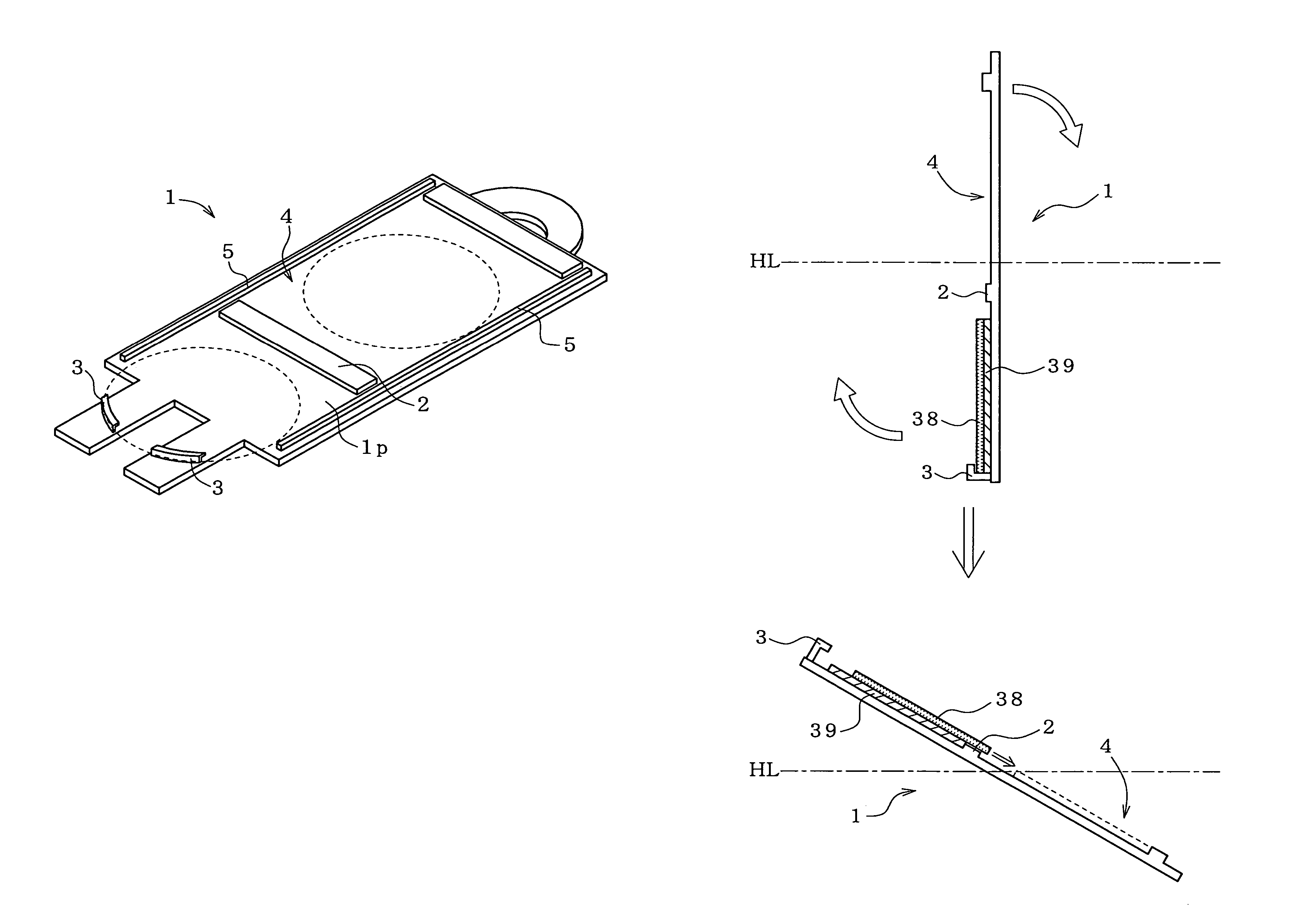
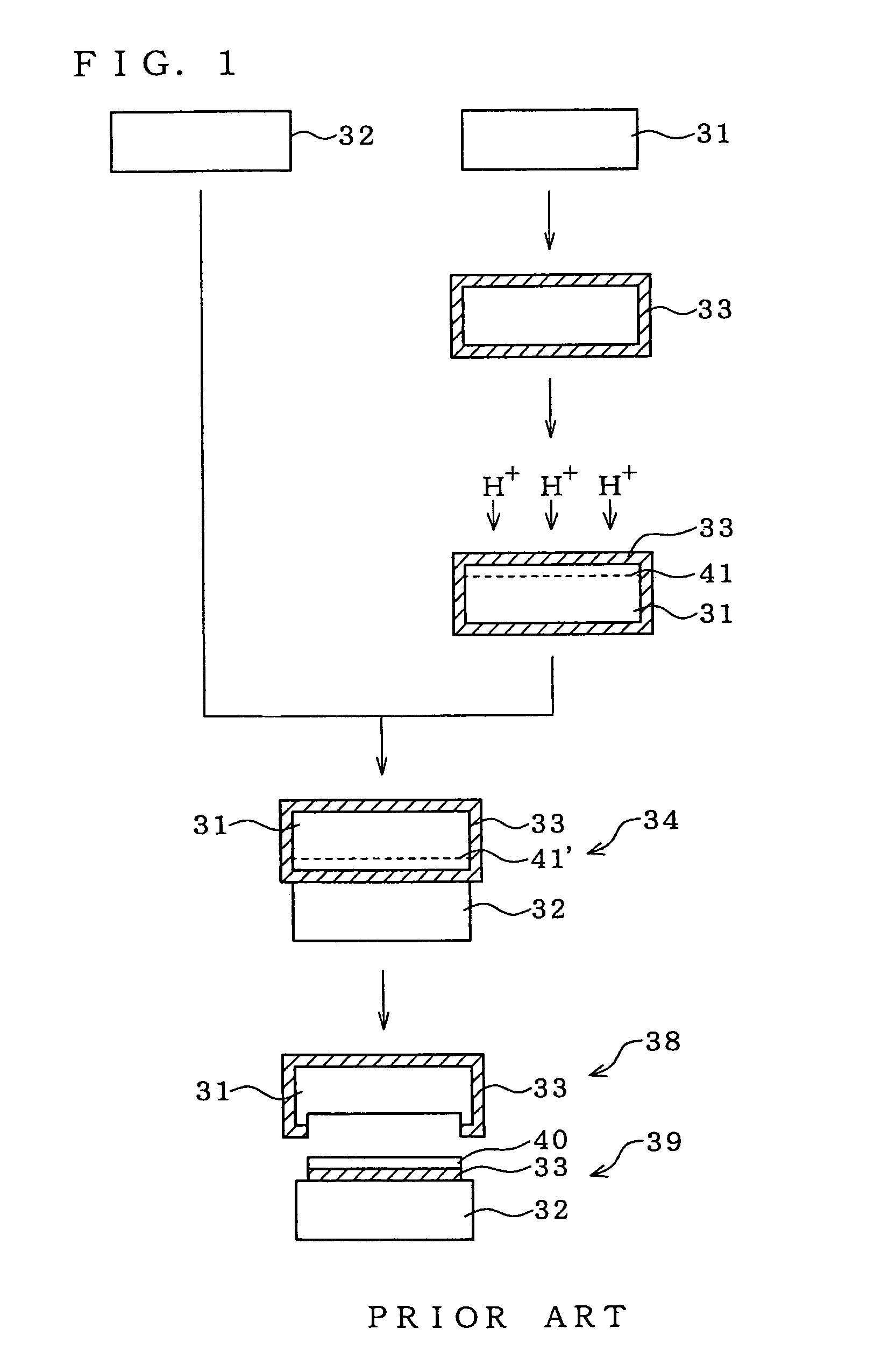
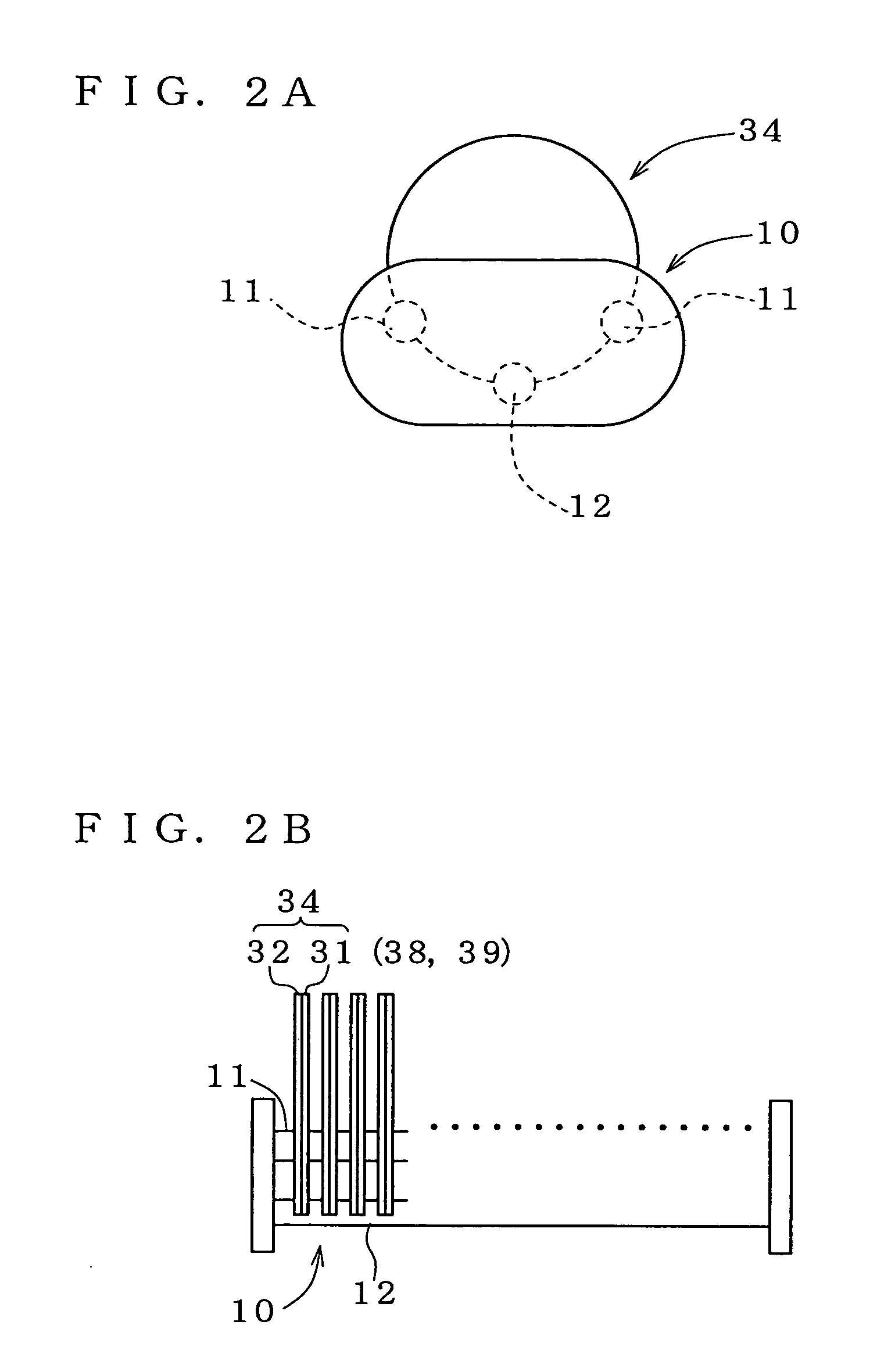
[0049]Experiments described below were carried out to confirm the effects of this invention. First, silicon single crystal wafers having a crystal orientation of the main surface of (100), a resistivity of 10 Ω·cm, and a diameter of 200 mm were obtained, and a plurality of SOI wafers 39 were fabricated according to the method shown in FIG. 1. The thickness of the oxide film 33 on the bond wafer 31 was 145 nm, and through which H+ ions were implanted under the conditions of an acceleration voltage of 56 keV and a dosage of 5.5×1016 cm−2. Under these conditions, the SOI layer 40 of approximately 340 nm thick was formed. The annealing was carried out using the boat 10 having a form as shown in FIG. 2, and in an inert atmosphere of an Ar / N2 mixed gas at 500° C. for 30 minutes. The boat 10 was then taken out from the annealing furnace, and the SOI wafers 39 and the residual wafers 38 were separated and recovered according to the method of using the vacuum chuck 36 as shown in FIG. 7. The...


PUM


Abstract

In the process of fabricating an SOI wafer based on the Smart Cut® Process, a stack 34 of an SOI wafer 39 and a residual wafer 38 are separated into the individual wafers using a wafer separation jig 1 of this invention. The wafer separation jig 1 comprises a supporting plane 1p on which the stack 34 is supported in the thickness-wise direction, and a stepped portion 2 disposed on the supporting plane 1p, and having a height adjusted so as to stop movement-by-sliding of the lower wafer of the stack, but so as to allow movement-by-sliding of the upper wafer relative to the lower wafer. Both wafers are separated from each other by inclining the supporting plane 1p with the stack 34 placed thereon, so as to allow the upper wafer to move by sliding as being driven by its own weight in the in-plane direction relative to the lower wafer. This method is successful in effectively suppressing friction between the wafers, and thus in preventing the wafer surface from being scratched.

Description

TECHNICAL FIELD[0001]This invention relates to a method of fabricating an SOI wafer and a wafer separation jig used therefor.BACKGROUND ART[0002]Bonding method is a well-known representative method for fabricating an SOI wafer (Silicon on Insulator) which comprises an insulating layer such as a silicon oxide film, and a silicon single crystal layer formed as being stacked thereon. Among others, ion implantation delamination method, so-called Smart Cut® Process (registered trademark) has been attracting a public attention, in which a silicon single crystal is implanted with ions and then annealed, so as to partially break the crystal lattice of silicon at the layer where the implanted ions reside, to thereby form an SOI layer.[0003]In the Smart Cut Process® shown in FIG. 1, a bond wafer 31 having an ion implanted layer 41 formed therein and a base wafer 32 on which an SOI layer 40 is to be formed later are annealed as being closely contacted with each other while placing in between a...

Claims


Application Information

Patent Timeline
Patent Type & Authority Patents(United States)
IPC IPC(8): H01L21/30B65G49/07H01L21/677H01L21/00H01L21/02H01L21/68H01L21/762H01L27/12
CPCH01L21/67092H01L21/76254Y10S414/135
Inventor AGA, HIROJITAKAHASHI, HIROYUKIMITANI, KIYOSHI
Owner SHIN-ETSU HANDOTAI CO LTD
Why Eureka
Try Eureka