High frequency device

a high-frequency device and device technology, applied in the direction of fixed capacitor details, waveguides, fixed capacitors, etc., can solve the problems of weak mechanical strength of the foregoing membrane structure (thin film structure), further decrease of strength, and difficulty in chip handling in mounting, so as to improve mechanical strength, strengthen structure, and increase mechanical strength of the dielectric layer as a device formation layer

Active Publication Date: 2011-03-03
SONY SEMICON SOLUTIONS CORP
View PDF2 Cites 0 Cited by
  • Summary
  • Abstract
  • Description
  • Claims
  • Application Information

AI Technical Summary

Benefits of technology

In the second high frequency device, by the reinforced structure in the aperture that is integrated with the substrate, mechanical strength of the dielectric layer as a device formation layer is increased.
According to the first high frequency device of the embodiment of the invention, the first dielectric layer as the stopper layer is provided between the substrate and the second dielectric layer as the element formation layer. Thus, the element formation layer (second dielectric layer) is able to be prevented from being damaged by etching in forming the aperture in the substrate. Therefore, mechanical strength is improved, and the manufacturing yield ratio is improved.
According to the second high frequency device of the embodiment of the invention, the reinforced structure integrated with the substrate is provided in the aperture of the substrate, and inside of the aperture is divided into the plurality of regions. Thus, as in the first high frequency device, mechanical strength of the element formation layer (dielectric layer) is improved, and the manufacturing yield ratio is improved.

Problems solved by technology

However, in general, mechanical strength of the foregoing membrane structure (thin film structure) is weak.
Further, the strength is further decreased by damaging the membrane in etching for removing the substrate from the rear face thereof.
In particular, in the case where the designed film thickness of the membrane is small or the area thereof is large, chip handling in mounting becomes difficult, and in addition, membrane self-support itself is in trouble.
To resolve such an event, there is a disadvantage that wiring design dimensions should be increased, for example, the thickness of the membrane should be increased.

Method used


Image

  • High frequency device
  • High frequency device
  • High frequency device

Examples


first embodiment

(1) Whole configuration

(2) Manufacturing method

Second embodiment

Whole configuration of a high frequency device having a reinforced structure

Third embodiment

High frequency device having an antenna as a high frequency element

Fourth embodiment

Mounting example

1. First embodiment

(1) Whole Configuration

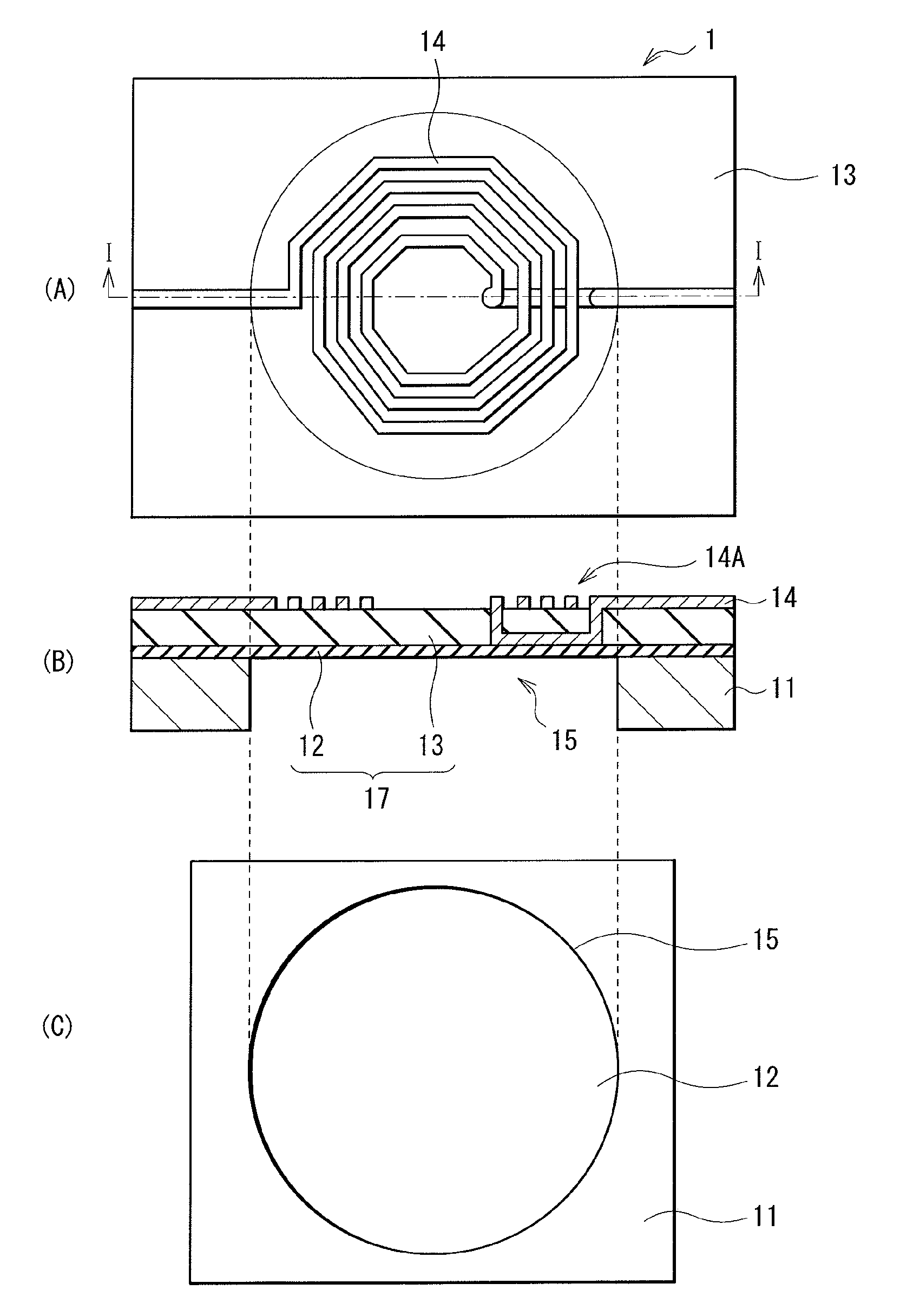
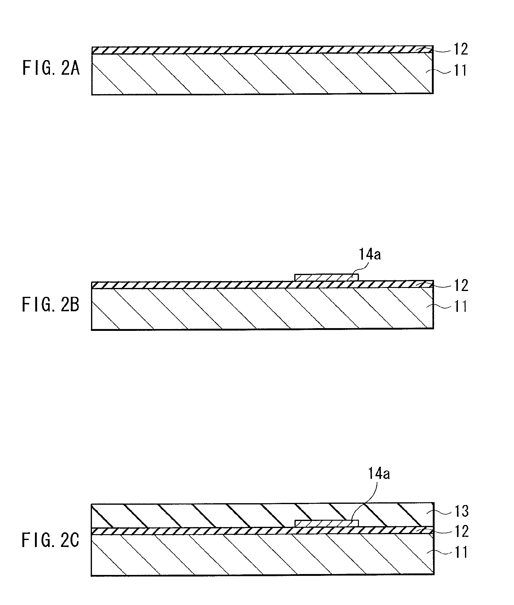
FIG. 1 illustrates a configuration of a high frequency device 1 according to a first embodiment of the invention. Part A in FIG. 1 illustrates a planar configuration of the high frequency device 1 viewed from the top face thereof. Part B in FIG. 1 illustrates a cross sectional structure taken along line I-I of part A in FIG. 1. Part C in FIG. 1 illustrates a planar configuration of the high frequency device 1 viewed from the bottom face thereof. The high frequency device 1 has a configuration in which a stopper layer 12 as a membrane and a dielectric layer 13 are layered in this order over a substrate 11. On the dielectric layer 13 (element formation layer), a high frequency element 14 is f...

second embodiment

FIG. 5 illustrates a cross sectional configuration of a high frequency device 2 according to a second embodiment of the invention. Part A in FIG. 5 illustrates a cross sectional configuration of the high frequency device 2. Part B and Part C in FIG. 5 illustrate a planar configuration of the high frequency device 2 viewed from the bottom face thereof. This embodiment is suitable for a case necessitating the membrane 17 (the stopper layer 12 and the dielectric layer 13) having a larger area. For the same elements as those of the first embodiment, the same referential symbols are affixed thereto and the descriptions thereof will be omitted.

The high frequency device 2 has the stopper layer 12, the dielectric layer 13, and the high frequency element 14 (inductor 14A) over the substrate 11 similarly in the first embodiment, but is different from the first embodiment in that the high frequency device 2 has a reinforced structure 18 in the aperture 15. The reinforced structure 18 is integr...

third embodiment

FIG. 6 illustrates a high frequency device 3 according to a third embodiment. Part A in FIG. 6 illustrates a planar configuration of the high frequency device 3 viewed from the top face thereof. Part B in FIG. 6 illustrates a cross sectional configuration taken along line II-II of Part A in FIG. 6. Part C in FIG. 6 illustrates a planar configuration of the high frequency device 3 viewed from the bottom face thereof.

The high frequency device 3 includes an antenna 14B as the high frequency element 14. The antenna 14B is an inverted F on-chip antenna composed of a linear radiating element 14d, an electric supply line 14e to supply electric power to the radiating element 14d, and a GND region 14E The reinforced structure 18 has a pattern perpendicular to the longitudinal direction of the radiating element 14d, and divides the radiating device 14d into a plurality of regions. Thereby, while influence on directivity and frequency change of the antenna 14B is suppressed, strength of the me...


PUM

PropertyMeasurementUnit
frequencyaaaaaaaaaa
resonance frequencyaaaaaaaaaa
frequencyaaaaaaaaaa

Abstract

A high frequency device having a membrane structure with improved mechanical strength is provided. The high frequency device includes: a substrate having an aperture; a first dielectric layer that is formed from a material having etching selectivity in relation to a material of the substrate and is provided on the substrate to cover the aperture; a second dielectric layer on the first dielectric layer; and a high frequency element provided in a position opposed to the aperture on the second dielectric layer.

Description

BACKGROUND OF THE INVENTION1. Field of the InventionThe present invention relates to a high frequency device used for MEMS (Micro Electro Mechanical Systems).2. Description of the Related ArtAlong with miniaturization of Si-CMOS (Complementary Metal Oxide Semiconductor), transistor shielding frequency has been drastically improved up to 100 GHz or more. Thereby, it is needless to say that application to several GHz band mainly used in current wireless devices is enabled, and in addition, it is prospective that application to 60 GHz or more millimeter waveband will be enabled. Such an application is a so-called RF-CMOS circuit. By integrating a base band section and an RF front end section into one chip by the CMOS, largely lowered cost is allowed to be realized, and thus active development of the RF-CMOS circuit has been made.One of tasks in developing the RF-CMOS circuit is, for example, an inductor. In the RF-CMOS, an Si substrate having lower resistance (from several to several k...

Claims


Application Information

Patent Timeline
Patent Type & Authority Applications(United States)
IPC IPC(8): H01P3/08H01F5/00H01L23/12H01P11/00
CPCH01F2017/0046H01F17/0006H01L2224/16225
Inventor MITARAI, SHUNTONOSAKI, MINEHIROIKEDA, KOICHI
Owner SONY SEMICON SOLUTIONS CORP
Why Eureka
Try Eureka