Shift register and method of driving the same

Active Publication Date: 2006-02-21
SEMICON ENERGY LAB CO LTD
View PDF13 Cites 26 Cited by
  • Summary
  • Abstract
  • Description
  • Claims
  • Application Information

AI Technical Summary

Benefits of technology

[0072]With the above structure, a shift register which does not malfunction and which can operate at hig

Problems solved by technology

However, the following problems arise because the amplitude voltage of clock pulse CK and inverted clock pulse CKB is smaller than the power supply voltage.
When the leak current is large, it is impossible to make pulses of outputs SB shift.
In this way, the shift register cannot perform output normally to be likely to malfunction when the TFTs that should remain OFF are turned ON.
In addition, power consumption is large because the wiring capacitance and wiring resistance are large at a connection portion between the level shifter and the circuits on the panel substrate.
On the other hand, if the level shifter is f

Method used


Image

  • Shift register and method of driving the same
  • Shift register and method of driving the same
  • Shift register and method of driving the same

Examples


Example

[Embodiment 1]

[0102]A circuit diagram, which is equivalent to the circuit diagram of FIG. 4 as an example of prior art, is used to describe a shift register according to Embodiment 1 of the present invention. Identical components with those in FIG. 4 are denoted by the same reference symbols and explanations thereof are omitted.

[0103]The shift register of the present invention receives a start pulse SP and clock pulse CK with a smaller amplitude voltage than power supply voltage (corresponding to a electric potential difference between a high power supply electric potential Vdd and a low power supply electric potential Vss) of the shift register.

[0104]Here, each stage of the shift register has a first clocked inverter and a second clocked inverter. The second clocked inverter CKINV2 has p-channel TFTs 502a and 502b and their gate width is set to ½ or more of the gate width of p-channel TFTs 501a and 501b of the first clocked inverter.

[0105]The gate width of a TFT here refers to a le...

Example

[Embodiment 2]

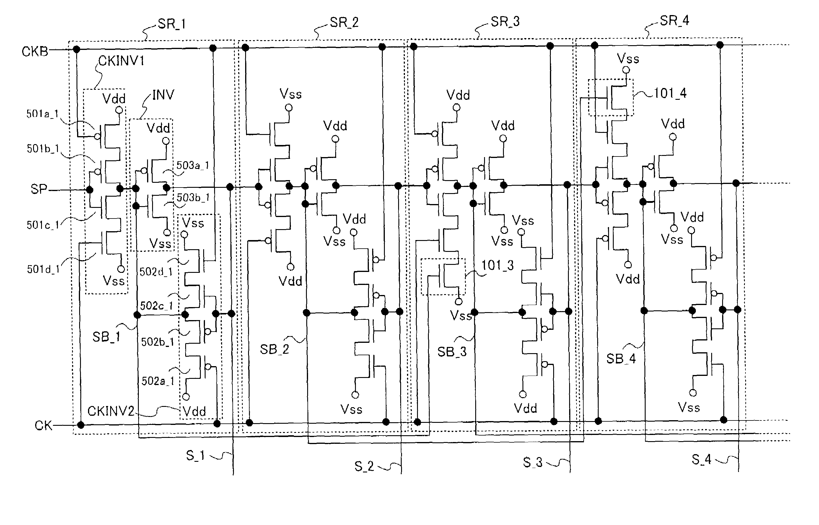
[0118]FIG. 1 is a circuit diagram which shows the structure of a shift register in Embodiment 2. Components of this shift register that are identical with those in FIG. 4 are denoted by the same reference symbols and explanations thereof are omitted.

[0119]The shift register of the present invention receives a start pulse SP and clock pulse CK with a smaller amplitude voltage than the power supply voltage (corresponding to the electric potential difference between the high power supply electric potential Vdd and the low power supply electric potential Vss) of the shift register. The above causes leak current of a first clocked inverter. This embodiment reduces the leak current by the following structure.

[0120]In FIG. 1, an n-channel TFT 101 is added to the first clocked inverter CKINV1 in the third stage that constitutes the shift register and in each of the subsequent stages to the third stage. The n-channel TFT 101 in the k-th (k is a natural number equal to or larger...

Example

[Embodiment 3]

[0138]This embodiment describes a shift register structured differently from Embodiment 2 illustrated in FIG. 1. The description will be given with reference to FIG. 8. In FIG. 8. identical components with those in FIG. 1 are denoted by the same reference symbols and explanations thereof will be omitted.

[0139]The shift register of the present invention receives a start pulse SP and clock pulse CK with a smaller amplitude voltage than the power supply voltage (corresponding to the electric potential difference between the high power supply electric potential Vdd and the low power supply electric potential Vss) of the shift register. The above causes a leak current of a first clocked inverter. This embodiment reduces the leak current by the following structure.

[0140]In FIG. 8, the n-channel TFT 101 is added to the first clocked inverter CKINV1 in the second stage that constitutes the shift register and in each of the subsequent stages to the second stage. The n-channel T...


PUM


Abstract

A clock pulse with a smaller amplitude voltage than the power supply voltage of the shift register is inputted to the shift register. The gate width of a TFT that constitutes a second clocked inverter of the shift register is set wide so as to reduce fluctuation in output electric potential due to leak current of a first clocked inverter. Further, a TFT is added to a first clocked inverter. A signal with an amplitude voltage of the same level as the power supply voltage is inputted to a gate electrode of the added TFT to switch between ON and OFF. The leak current of the first clocked inverter is thus cut off.

Description

BACKGROUND OF THE INVENTION[0001]1. Field of the Invention[0002]The present invention relates to a shift register. Specifically, the present invention relates to a shift register composed of thin film transistors (hereinafter referred to as TFTs) and to a method of driving the shift register.[0003]2. Description of the Related Art[0004]Shift registers, which receive a clock pulse and a start pulse to output pulses (sampling pulses) sequentially, are used in various circuits. In a display device which has a plurality of pixels arranged to form a matrix, shift registers are particularly used as a gate signal line driving circuit and a gate signal line driving circuit for selecting pixels and inputting signals to the selected pixels.[0005]An example of the structure of a general shift register is shown in FIG. 5. The shift register has first to r-th (r is a natural number equal to or larger than 3) stages. Each stage is composed of a first clocked inverter CKINV1, a second clocked inve...

Claims


Application Information

Patent Timeline
IPC IPC(8): G09G3/36G02F1/133G09G3/20G11C19/00G11C19/28
CPCG11C19/28G11C19/00G02F1/133
Inventor OSAME, MITSUAKI
Owner SEMICON ENERGY LAB CO LTD
Why Eureka
Try Eureka