Process and structure for semiconductor package

a technology of semiconductor packaging and process, applied in the direction of semiconductor/solid-state device details, semiconductor devices, electrical devices, etc., can solve the problems of incomplete removal of carriers, over-removal of metallic contact surfaces, and contamination of metal surfaces

Active Publication Date: 2006-02-28
ADVANCED SEMICON ENG INC
View PDF6 Cites 80 Cited by
  • Summary
  • Abstract
  • Description
  • Claims
  • Application Information

AI Technical Summary

Benefits of technology

[0009]Accordingly, one object of the present invention is to provide a packaging process capable of producing a package having the ad

Problems solved by technology

Since the carrier is made from copper, the etched away copper material may leak into the surroundings causing metallic contamination.
In addition, if the etching solution is improperly mixed or the ingredients thereof are slightly out of proportion, either the carrier is incompletely removed or the metallic contact surface is over-removed.
Meanwhile, each reflow operation causes some warpage of the film.
In addition, since the f

Method used


Image

  • Process and structure for semiconductor package
  • Process and structure for semiconductor package
  • Process and structure for semiconductor package

Examples


second embodiment

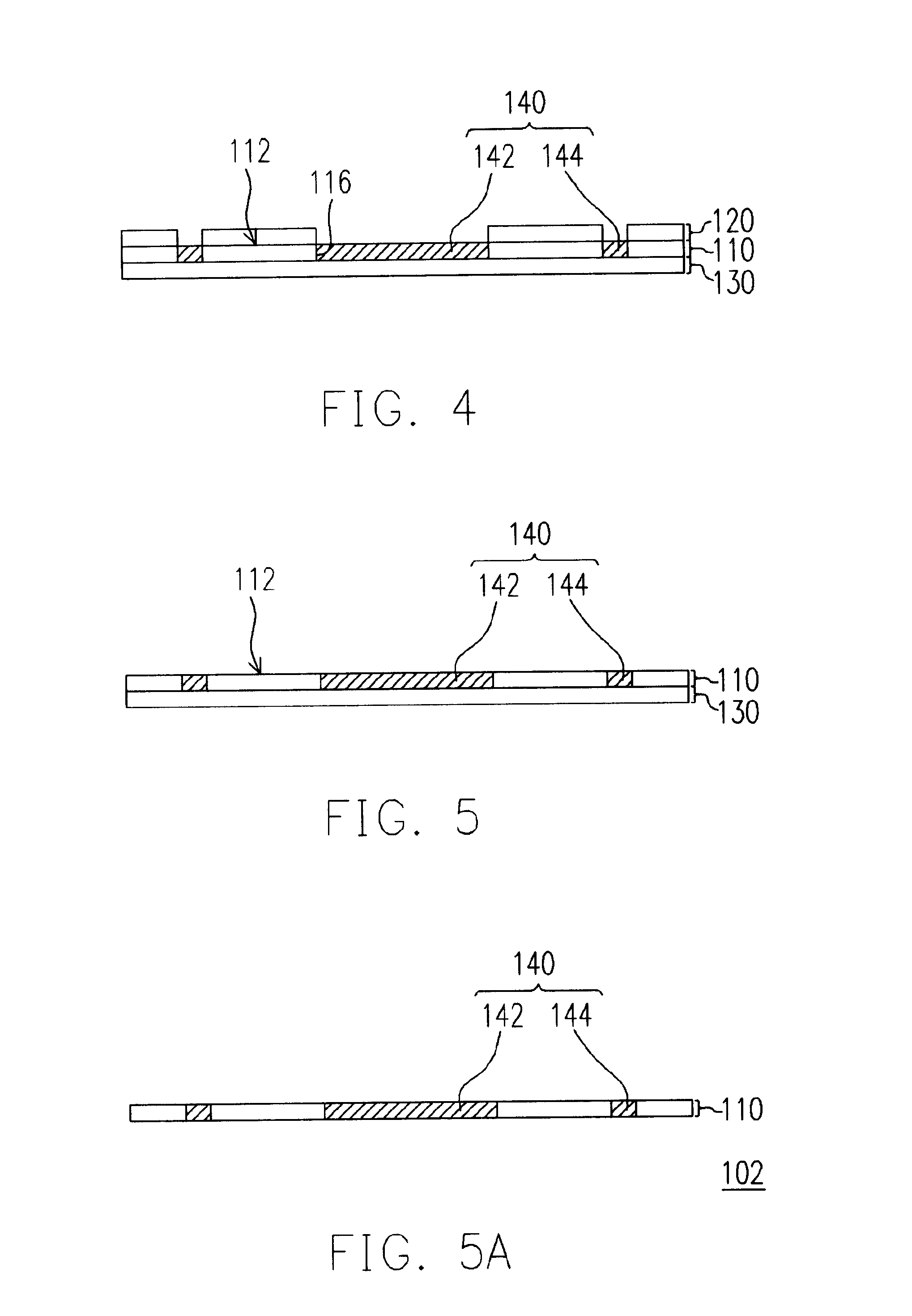
[0033]In the aforementioned embodiment, the substrate is a single-layered structure with the chip and the substrate electrically connected through conductive wires. However, the scope of this invention is not limited to this application. In this invention, the substrate is a multi-layered carrier and the chip and the substrate are electrically connected through bumps.

[0034]FIGS. 12 to 18 are schematic cross-sectional views showing the progression of steps in a packaging process according to a second preferred embodiment of this invention. First, as shown in FIG. 12, a carrier 110, a tape 130 and a conductive body 140 are formed using the processes as shown in FIGS. 1 to 5. Thereafter, an additional carrier 310, such as an additional insulation layer, is formed over the upper surface 112 of the carrier 110 by conducting a heat-pressing or spin-coating operation. The additional carrier 310 is made from a material, such as glass epoxy resin, Bismaleimide-Triazine, polyimide or epoxy re...

first embodiment

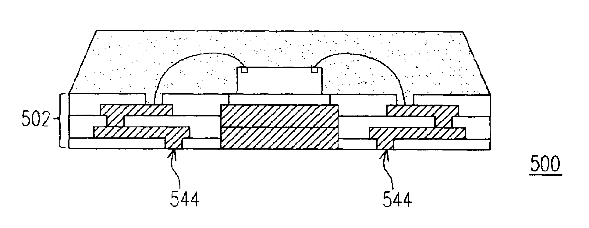
[0039]The tape 130 may remain attached to the substrate 502 until the final of the packaging process. The subsequent steps for fabricating the structure as shown in FIG. 26 is similar to this invention, and the detailed description is not repeated. Finally, the tape 130 is removed from the lower surface 114 of the carrier 110 to form a package structure 500 as shown in FIG. 27. Since the tape 130 is removed from the carrier 110 in the last step, surface contamination of the contacts 544 is reduced. The package 500 can be later attached to a printed circuit board (not shown) using a surface mount technology. The printed circuit board connects electrically with the package 500 through its contacts 544.

[0040]In conclusion, major advantages of this invention include: 1. Since the packaging process demands no metallic etching operation, environmental pollution is greatly reduced. 2. Since only one reflow step is required, the warpage level of the substrate is reduced. Ultimately, the sur...


PUM


Abstract

A packaging process for a semiconductor chip that includes the following steps. A carrier having an upper surface and a corresponding lower surface is provided. A photoresist layer is formed on the upper surface of the carrier. A plurality of photoresist openings that expose the carrier is formed in the photoresist layer. A plurality of openings that connects with the photoresist openings are formed in the carrier. A tape is attached to the lower surface of the carrier. The body is filled into the openings of the carrier. A chip is mounted onto the upper surface of the carrier and electrically connected therewith. Finally, the tape is removed from the lower surface of the carrier.

Description

CROSS REFERENCE TO RELATED APPLICATIONS[0001]This application claims the priority benefit of Taiwan application serial no. 91120701, filed on Sep. 11, 2002.BACKGROUND OF INVENTION[0002]1. Field of Invention[0003]The present invention relates to a package process and structure. More particularly, the present invention relates to a semiconductor packaging process and a structure having an improved processing reliability.[0004]2. Description of Related Art[0005]In this information age, electronic products have become indispensable tools in every part of our daily life. At the core of each electronic product is usually a silicon chip that connects with other chips or passive electrical devices through a substrate. Since the chip is firmly attached as well as electrically connected to the substrate through a packaging process, a number of packaging structures have been developed such as bump chip carrier (BCC) package, film package and quad flat no-lead (QFN) package. All these packages ...

Claims


Application Information

Patent Timeline
IPC IPC(8): H01L21/44H01L21/48H01L21/68H01L23/31H01L23/498
CPCH01L21/4857H01L24/29H01L21/568H01L21/6835H01L23/3128H01L23/49822H01L23/49827H01L21/486H01L24/32H01L2221/68345H01L2224/32188H01L2224/32225H01L2224/48091H01L2224/48227H01L2224/48228H01L2224/73265H01L2224/83192H01L2224/92247H01L2924/01029H01L2924/01046H01L2924/01078H01L2924/01079H01L2924/01082H01L2924/15174H01L2924/10253H01L2224/73204H01L2224/16225H01L2224/16235H01L24/48H01L2924/01033H01L2924/00014H01L2924/00H01L2224/05599H01L2224/45099H01L2224/85399H01L2924/181H01L2924/00012H01L2224/45015H01L2924/207
Inventor KUNG, WEI-CHUNCHANG, LIAMH-CHENG
Owner ADVANCED SEMICON ENG INC
Why Eureka
Try Eureka