Schottky barrier transistor and method of manufacturing the same

Inactive Publication Date: 2006-02-28
ELECTRONICS & TELECOMM RES INST
View PDF8 Cites 3 Cited by
  • Summary
  • Abstract
  • Description
  • Claims
  • Application Information

AI Technical Summary

Benefits of technology

[0011]The present invention provides a SB transistor having optimal electrical characteristics as a result of eliminating the requirement for selective wet etching and decreasing etching damage.
[0012]The present invention also provides a method of manufacturing a SB transistor capable of eliminating the requirement for selective wet etching and decreasing etching damage.
[0015]According to the present invention, a polycrystalline silicon layer is formed on the top of a gate using a selective silicon growth. The polycrystalline silicon layer covers an upper surface and upper edges of the gate. Therefore, a spacer produces a shadow area, i.e., an area on which a metal for silicidation is not deposited. Since the shadow area electrically insulates the gate and the source / drain, a selective wet etching process for removing an unreacted metal can be omitted. In addition, a monocrystalline silicon layer grown on a substrate can decrease etching damage caused during spacer etching.

Problems solved by technology

However, integration simply by reduction in transistor size causes various problems.
The most important issues are a short channel effect (SCE) due to the scaling-down of devices and a source / drain doping associated with a decrease in source / drain resistance.
In particular, the formation of a source / drain by ion implantation in a conventional transistor fabrication method is accompanied by the following problems.
First, it is difficult to adjust the depth of a junction.
Since diffusion of impurities occurs both in depth and channel directions, it is difficult to prevent a short channel effect.
However, a channel depth of less than 10 nm for prevention of a short channel effect is difficult to attain.
Second, a saturation current is unavoidably reduced.
Therefore, a metal gate cannot be used.
Fourth, a soft error rate at a junction interface is high and a floating body effect may be caused.
However, since interest in using SB transistors as alternatives to nanoelectronic devices have been raised just recently, optimization of the structure and fabrication process of the SB transistors has still not been established.
In particular, one important and difficult process in the SB transistor fabrication method is selective wet etching for removing only an unreacted metal.
However, use of noble metals and formation of a fine pattern increase the difficulty of the selective wet etching.
Another important and difficult process in the SB transistor fabrication method is etching damage removal.
Etching damage caused during a formation of a spacer on a sidewall of a gate is a main factor that adversely affects the interface characteristics between the metal silicide layer and the silicon substrate.
Until now, there have been no efficient solutions to the etching damage.

Method used


Image

  • Schottky barrier transistor and method of manufacturing the same
  • Schottky barrier transistor and method of manufacturing the same
  • Schottky barrier transistor and method of manufacturing the same

Examples


Embodiment Construction

[0020]The present invention will now be described more fully with reference to the accompanying drawings in which preferred embodiments of the invention are shown. This invention may, however, be embodied in many different forms and should not be construed as being limited to the embodiments set forth herein. Rather, these embodiments are provided so that this disclosure will be thorough and complete, and will fully convey the scope of the invention to those skilled in the art. In the drawings, the forms of elements are exaggerated for clarity. To facilitate understanding, identical reference numerals have been used, where possible, to designate identical elements that are common to the figures.

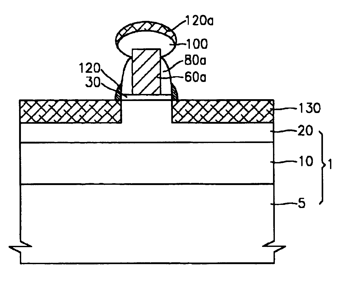
[0021]FIG. 1 is a sectional view of a SB transistor according to an embodiment of the present invention. Referring to FIG. 1, entire structures are formed on a silicon on insulator (SOI) wafer 1. The SOI wafer 1 has a sequentially stacked structure of a base silicon layer 5, a buried oxide la...


PUM


Abstract

A schottky barrier transistor and a method of manufacturing the same are provided. The method includes forming a gate insulating layer and a gate on a substrate, forming a spacer on a sidewall of the gate, and growing a polycrystalline silicon layer and a monocrystalline silicon layer on the gate and the substrate, respectively, using a selective silicon growth. A metal is deposited on the polycrystalline silicon layer and the monocrystalline silicon layer. Then, the metal reacts with silicon of the polycrystalline silicon layer and the monocyrstalline silicon layer to form a self-aligned metal silicide layer. Therefore, selective wet etching for removing an unreacted metal after silicidation can be omitted. Furthermore, etching damage caused during the formation of the spacer can be decreased during the growth of the monocrystalline silicon layer, thereby improving the electrical characteristics of devices.

Description

BACKGROUND OF THE INVENTION[0001]This application claims priority from Korean Patent Application No. 2003-23969, filed on Apr. 16, 2003, in the Korean Intellectual Property Office, the disclosure of which is incorporated herein by reference in its entirety.[0002]1. Field of the Invention[0003]The present invention relates to a transistor and a method of manufacturing the same. More particularly, the present invention relates to a schottky barrier transistor (referred to as “SB transistor”, hereinafter) using a schottky barrier formed between a metal and a semiconductor, and a method of manufacturing the same.[0004]2. Description of the Related Art[0005]Semiconductor device fabrication technology has reached the level where it is now possible to fabricate transistors that have a short channel with a length less than 100 nm. However, integration simply by reduction in transistor size causes various problems. The most important issues are a short channel effect (SCE) due to the scaling...

Claims


Application Information

Patent Timeline
IPC IPC(8): H01L21/28H01L21/336H01L29/872H01L29/47H01L29/78H01L29/786H01L29/812
CPCH01L21/28114H01L21/28123H01L29/665H01L29/78654H01L29/66643H01L29/7839H01L29/66636H01L29/812
Inventor CHEONG, WOO SEOKLEE, SEONG JAEJANG, MOON GYU
Owner ELECTRONICS & TELECOMM RES INST
Why Eureka
Try Eureka