Adaptive bias circuit for a power amplifier

a bias circuit and power amplifier technology, applied in the direction of amplifiers with semiconductor devices only, amplifiers with semiconductor devices/discharge tubes, gain control, etc., can solve the problems of difficult installation of components such as rf couplers/envelope detectors and dc-to-dc converters within, and the conventional power amplifier operates at a relatively low output. , to achieve the effect of effectively controlling dc power consumption, improving power added efficiency, and cost-effective and mini

Inactive Publication Date: 2006-02-28
INFORMATION & COMM UNIV EDUCATIONAL FOUND
View PDF9 Cites 23 Cited by
  • Summary
  • Abstract
  • Description
  • Claims
  • Application Information

AI Technical Summary

Benefits of technology

[0008]It is, therefore, an object of the present invention to provide a cost-effective and miniaturized adaptive bias circuit capable of effectively controlling DC power consumption as the output power varies to thereby greatly improve a power added efficiency when the output power is low as well as maintaining a high linearity of the power amplifier when the output power is high.

Problems solved by technology

However, the conventional power amplifier usually operates at a relatively low output power ranging from, e.g., −15 to 15 dBm.
These conventional techniques, however, have a drawback in that it is very difficult to install such components as the RF coupler / envelope detector and the DC-to-DC converter within a highly miniaturized module of power amplifier having a size of, e.g., 6×6 mm2.

Method used


Image

  • Adaptive bias circuit for a power amplifier
  • Adaptive bias circuit for a power amplifier

Examples


Embodiment Construction

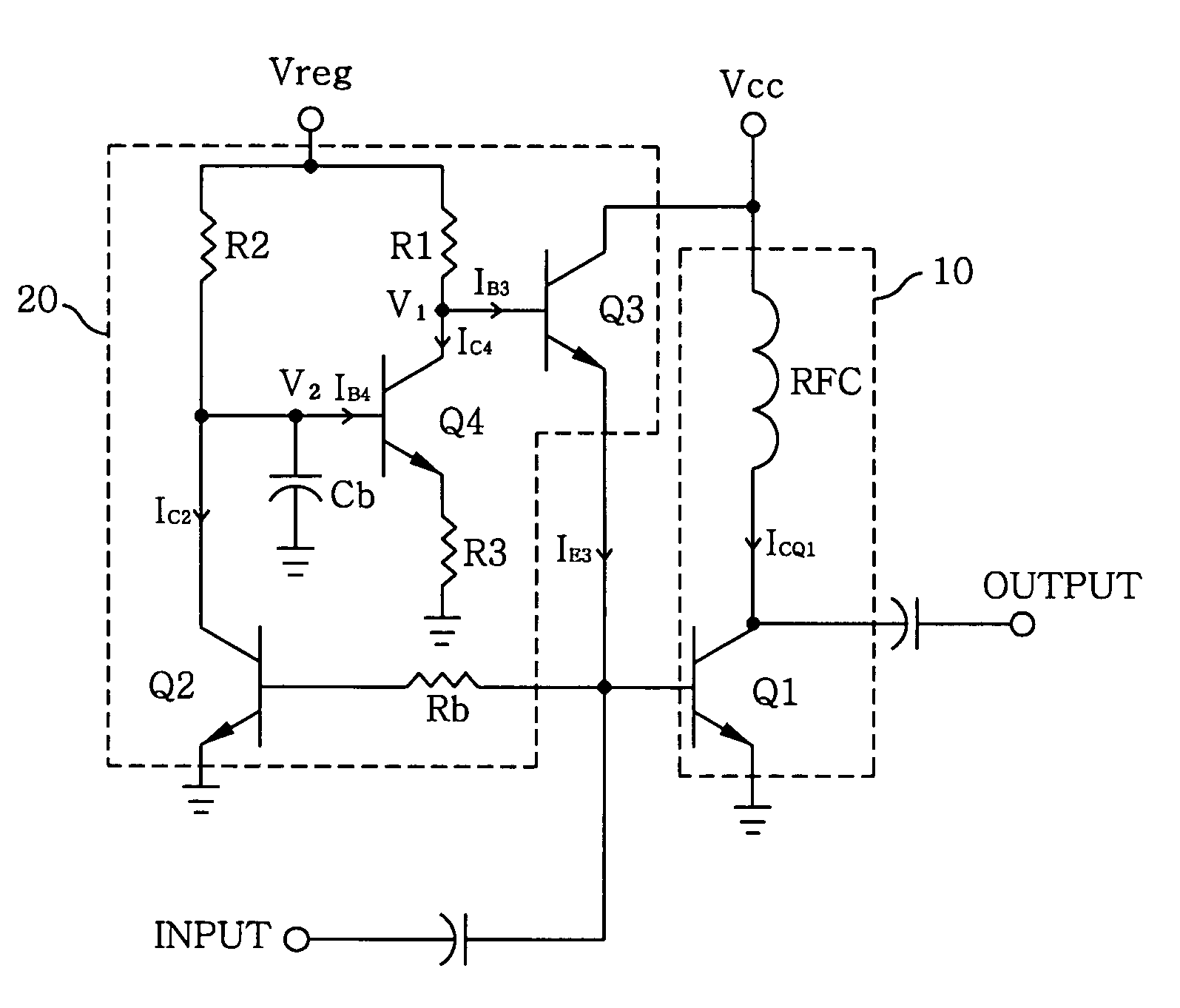
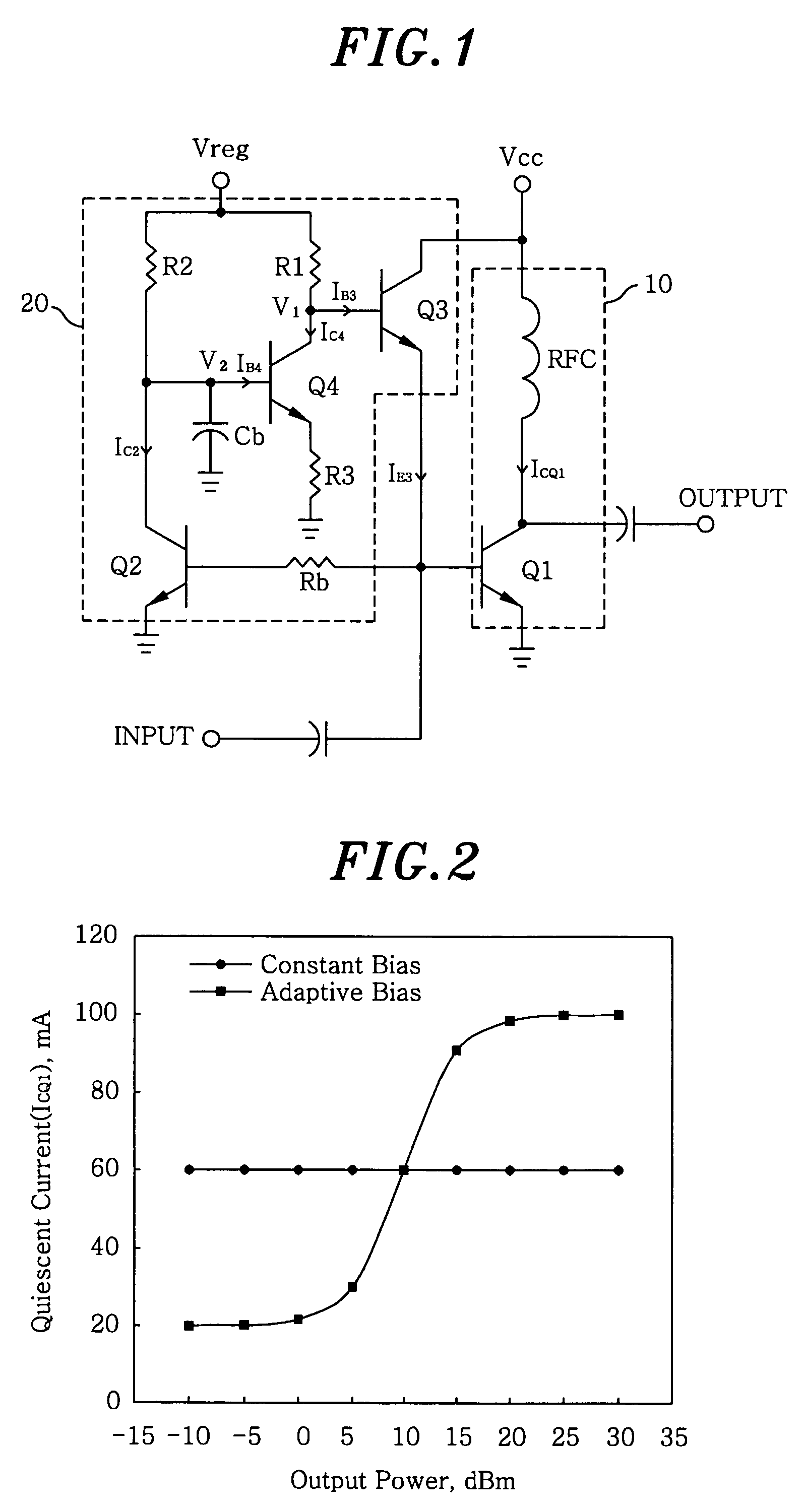
[0013]Referring to FIG. 1, there is provided a power amplifier module including an adaptive bias circuit in accordance with a preferred embodiment of the present invention. The power amplifier module includes an RF (radio frequency) power amplifier 10 having a first transistor Q1 and an RF choke inductor RFC; and an adaptive bias circuit 20 having a second transistor Q2, a third transistor Q3, a fourth transistor Q4, a bypass capacitor Cb, a base resistor Rb, a first bias resistor R1, a second bias resistor R2 and an emitter resistor R3. An input terminal of the power amplifier module is connected to both the RF power amplifier 10 and the bias circuit 20. A DC source voltage supply Vcc is connected to both the RF power amplifier 10 and the bias circuit 20 and a regulated voltage supply Vreg is connected to the bias circuit 20.

[0014]Functioning as a class-AB power amplifier, the RF power amplifier 10 receives an input signal from the input terminal, and amplifies the input signal to ...


PUM


Abstract

An adaptive bias circuit is provided for an amplifier module including a RF power amplifier for amplifying an input signal to generate an output signal, wherein the bias circuit receives the input signal to adjust a driving current to control a quiescent current of the RF power amplifier. The adaptive bias circuit includes means for providing the driving current to the bias circuit and means for drawing a bypass current from the providing means to reduce the driving current in response to the input signal, wherein the quiescent current is reduced when the driving current is reduced and the bypass current increases when the input signal is reduced.

Description

FIELD OF THE INVENTION[0001]The present invention relates to a bias circuit for an amplifier module; and, more particularly, to an adaptive bias circuit capable of improving a power added efficiency of a power amplifier when an output power is low as well as maintaining a high linearity of the power amplifier when the output power is high.BACKGROUND OF THE INVENTION[0002]In a wireless mobile communications system, a power amplifier is a key component that determines a lifetime of a battery in a mobile terminal, e.g., a conventional CDMA mobile handset. Thus, the power amplifier is required to be of a high efficiency characteristic in order to increase the lifetime of the battery. Since the power added efficiency of the conventional power amplifier is highest when an output power thereof is at its highest level, it lowers as the output power backs off at the highest level, e.g., 30 dBm. However, the conventional power amplifier usually operates at a relatively low output power rangin...

Claims


Application Information

Patent Timeline
Patent Type & Authority Patents(United States)
IPC IPC(8): H03G3/10H03F3/21H03F1/02H03F1/30H03F3/20H03G3/30
CPCH03F1/0261H03G3/3042H03F1/302H03F3/20
Inventor NOH, YOUN SUBPARK, CHUL SOON
Owner INFORMATION & COMM UNIV EDUCATIONAL FOUND
Why Eureka
Try Eureka