

Leadframe strip having enhanced testability
a testability and leadframe technology, applied in the direction of individual semiconductor device testing, semiconductor/solid-state device testing/measurement, instruments, etc., can solve the problems of affecting the reliability of solder mounting and joint, the leadframe is bursting, and the cost-intensive saw singulation blade is prematurely worn, so as to facilitate strip testing, facilitate the creation of various isolation cuts, and increase the design flexibility and integration of the semiconductor package
- Summary
- Abstract
- Description
- Claims
- Application Information
AI Technical Summary
Benefits of technology
Problems solved by technology
Method used
Image

Examples
Embodiment Construction
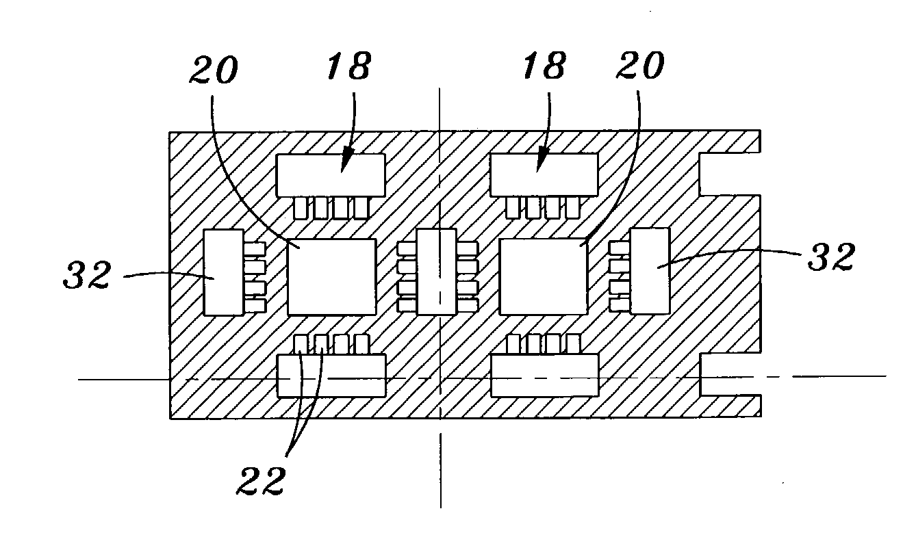
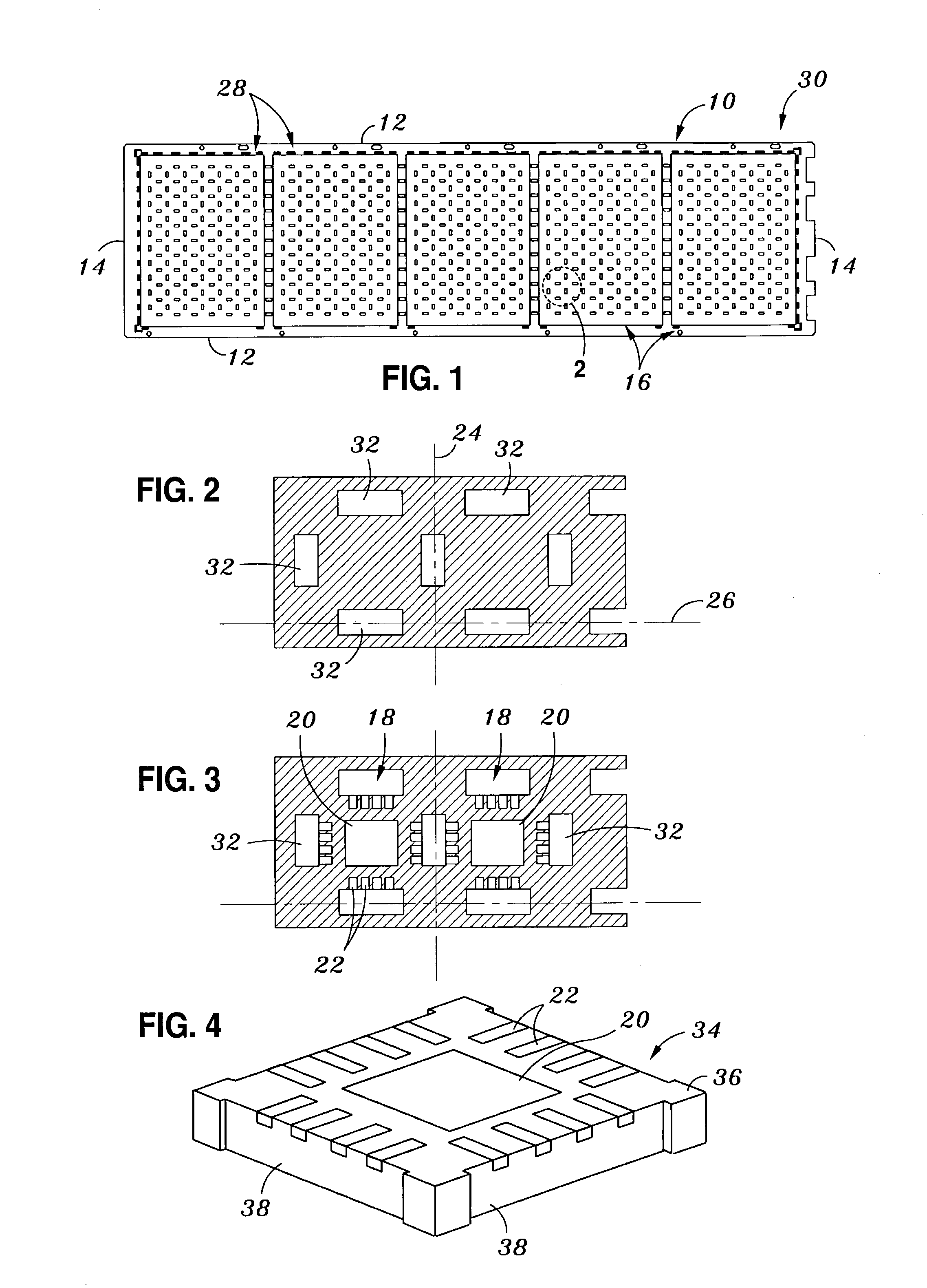
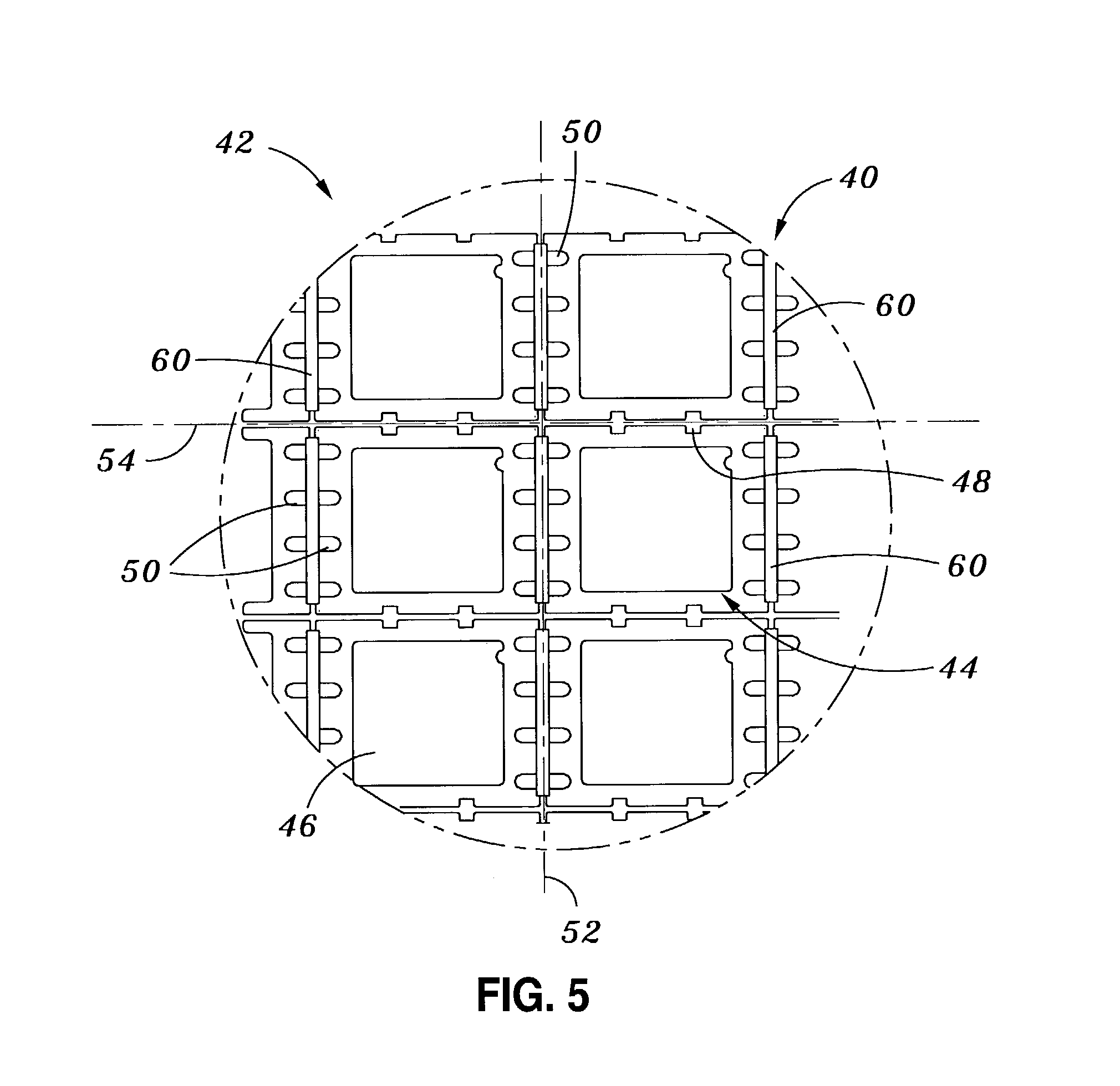
[0030]Referring now to the drawings wherein the showings are for purposes of illustrating preferred embodiments of the present invention only, and not for purposes of limiting the same, FIG. 1 depicts a leadframe strip 10 constructed in accordance with the present invention. The strip 10 has a generally rectangular configuration, defining an opposed pair of longitudinal peripheral edge segments 12 and an opposed pair of lateral peripheral edge segments 14. The strip 10 defines multiple identically configured arrays 16. Each array 16 defines a multiplicity of leadframes 18 which are best shown in FIG. 3.
[0031]Each leadframe 18 includes an outer frame portion which defines a centrally positioned opening. Disposed within the opening is a die pad 20 which has a generally quadrangular configuration. The die pad 20 is typically connected to the outer frame portion by a plurality of tie bars of the leadframe 18 which extend to the outer frame portion from respective ones of the corner regi...
PUM
 Abstract
Description
Claims
Application Information