Nitrogen passivation of interface states in SiO2/SiC structures

a technology of sio2/sic structure and interface state, which is applied in the direction of coatings, chemical vapor deposition coatings, semiconductor devices, etc., can solve the problems of reducing the performance of electronic devices that incorporate such interfaces, affecting the electrical functioning of devices, and affecting the electrical properties of electronic devices, etc., to reduce the breakdown field strength of oxide layers, and reduce the density of interface states

Inactive Publication Date: 2006-04-04
CREE INC
View PDF78 Cites 23 Cited by
  • Summary
  • Abstract
  • Description
  • Claims
  • Application Information

AI Technical Summary

Benefits of technology

[0009]In particular embodiments, the annealing is performed at a pressure less than atmospheric pressure and at a temperature greater than about 1000° C. but less than about 1400° C. for a time period sufficient to lower the density of interface states. Some embodiments of the invention can reduce interface state density beyond the levels reported for NO, N2O or NH3 nitridation alone without substantially reducing the breakdown field strength of the oxide layer. Some embodiments of the invention also can improve the uniformity of charge distribution in the oxide layer.

Problems solved by technology

Traps may also be produced by other types of lattice defects near the interface.
Unwanted energy states may impair the electrical properties of material near the SiO2 / SiC interface and may reduce the performance of electronic devices that incorporate such interfaces, such as MOSFETs, capacitors and other devices.
Traps may also impair the electrical functioning of a device by causing field termination and / or Coulomb scattering.
Local nonuniformities at the SiC surface also may result in an uneven distribution of charge near the interface.
Variation in surface potential may cause undesirable characteristics in electronic devices.
Although nitridation by growth and / or post-oxidation annealing using N2O and / or NO has been shown to be successful in reducing the density of interface states (DIT) in SiO2 / SiC structures while maintaining acceptable oxide strength, experimental results have shown an upper limit on the reduction of DIT that can be achieved through such techniques.

Method used


Image

  • Nitrogen passivation of interface states in SiO2/SiC structures
  • Nitrogen passivation of interface states in SiO2/SiC structures
  • Nitrogen passivation of interface states in SiO2/SiC structures

Examples


examples

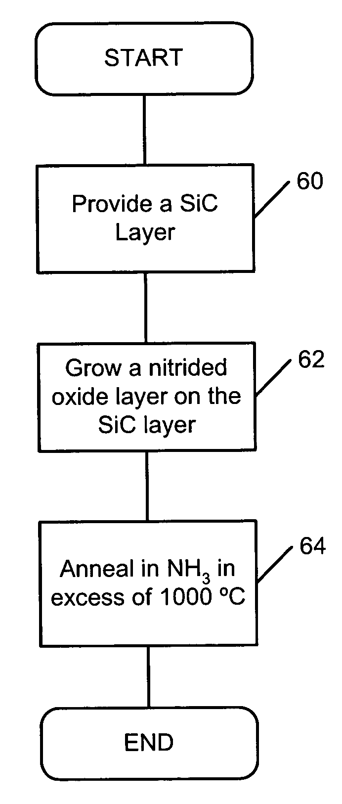
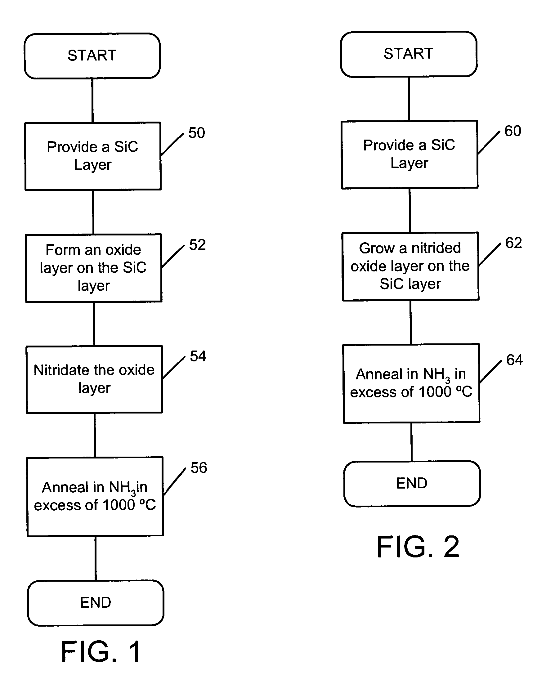
[0044]The following examples and experimental results shall be regarded as merely illustrative and shall not be construed as limiting the invention. In a first experiment, 450 Å thick layers of SiO2 were formed on 4H—SiC n-type wafers manufactured by Cree, Inc. by conventional dry oxidation techniques, including re-oxidation according to the process described in U.S. Pat. No. 5,972,801 issued Oct. 26, 1999 which is assigned to the assignee of the present invention and which is incorporated herein by reference as if fully set forth herein. The SiO2 / SiC interfaces were then nitrided according to the process described in U.S. patent application Ser. No. 09 / 834,283 filed Apr. 12, 2001 entitled “Method Of N2O Annealing An Oxide Layer On A Silicon Carbide Layer” referenced above. Specifically, the interface was annealed in a furnace tube at 1300° C. for 3 hours under an N2O flow rate of 4 SLM. Subsequently, the wafers were removed from the tube furnace.

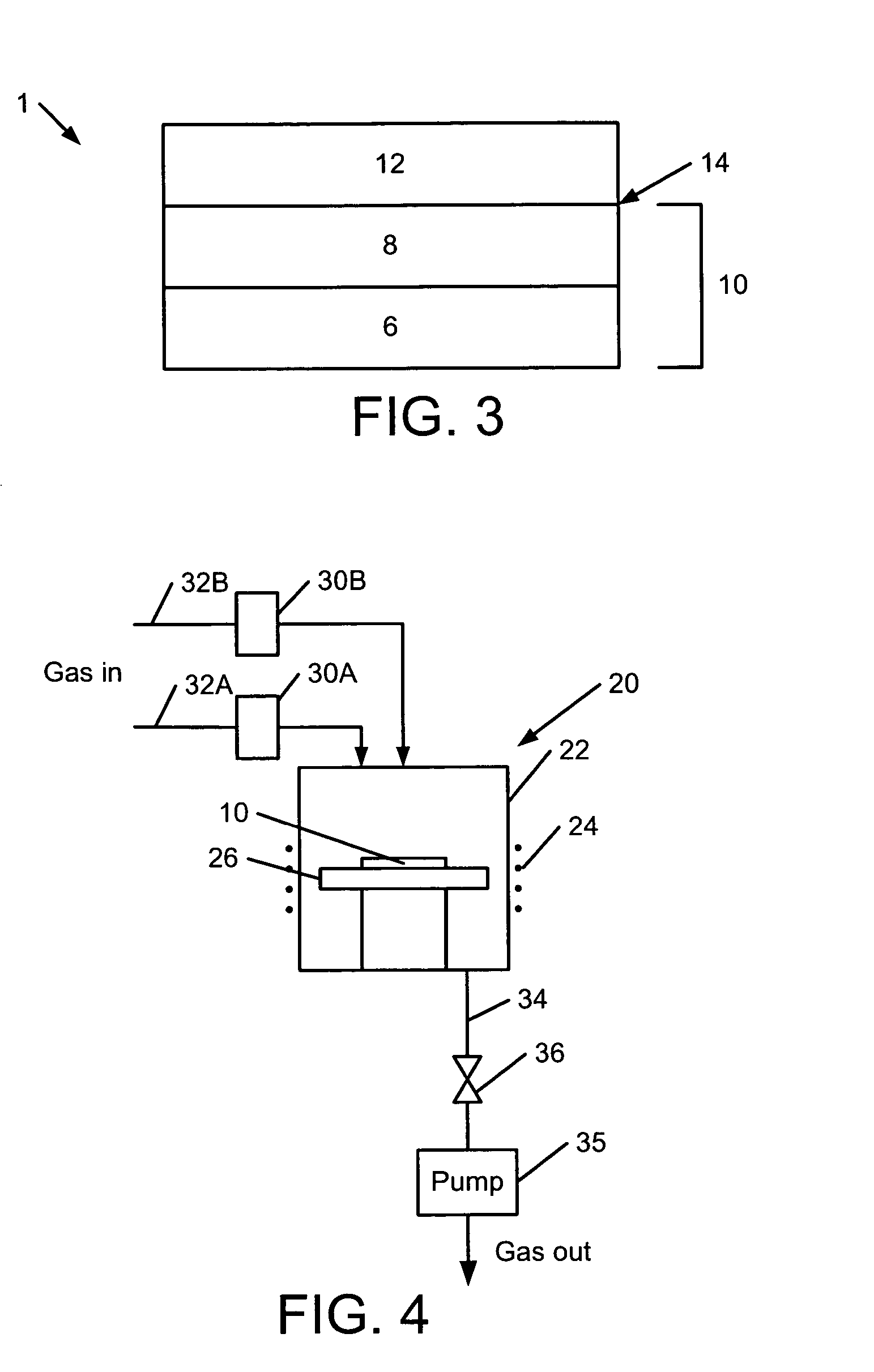
[0045]NH3 annealing was performed in...


PUM

PropertyMeasurementUnit
pressureaaaaaaaaaa
temperatureaaaaaaaaaa

Abstract

A nitrided oxide layer on a silicon carbide layer is processed by annealing the nitrided oxide layer in a substantially oxygen-free nitrogen containing ambient. The anneal may be carried out at a temperature of greater than about 900° C., for example, a temperature of about 1100° C., a temperature of about 1200° C. or a temperature of about 1300° C. Annealing the nitrided oxide layer may be carried out at a pressure of less than about 1 atmosphere, for example, at a pressure of from about 0.01 to about 1 atm or, in particular, at a pressure of about 0.2 atm. The nitrided oxide layer may be an oxide layer that is grown in a N2O and/or NO containing ambient, that is annealed in a N2O and/or NO containing ambient or that is grown and annealed in a N2O and/or NO containing ambient.

Description

RELATED APPLICATIONS[0001]The present application is related to and claims priority from U.S. Provisional Application Ser. No. 60 / 406,753, entitled “Nitrogen Passivation of Interface States in SiO2 / SiC Structures,” filed Aug. 30, 2002, the disclosure of which is incorporated herein in its entirety.STATEMENT OF GOVERNMENT SUPPORT[0002]The present invention was made with Government support under contract number N00014-02-C-0302 awarded by the Office of Naval Research. The Government has certain rights in this invention.BACKGROUND OF THE INVENTION[0003]Nitrogen passivation, also called “nitridation” is known to be an effective method for reducing the density of interface states at the SiO2 / SiC interface. Nitridation techniques, including growth and post-oxidation annealing are described in detail in U.S. patent publication no. 2002 / 0102358 published Aug. 1, 2002 entitled “Method Of Fabricating An Oxide Layer On A Silicon Carbide Layer Utilizing An Anneal In A Hydrogen Environment”, U.S...

Claims


Application Information

Patent Timeline
Patent Type & Authority Patents(United States)
IPC IPC(8): C23C16/40H01L21/04H01L21/318H01L21/314H01L29/78
CPCH01L21/049H01L21/3145H01L21/3143H01L21/022H01L21/02167H01L21/02332H01L21/02337H01L21/324
Inventor DAS, MRINAL KANTISAXLER, ADAM WILLIAM
Owner CREE INC
Why Eureka
Try Eureka