Method of fabricating a gate dielectric layer with reduced gate tunnelling current and reduced boron penetration

a dielectric layer and gate technology, applied in the field of gate dielectric layer fabrication, can solve the problems of high gate tunnelling current risk, degraded gate insulator layer as well as a dopant depleted gate structure, and gate insulator layers, etc., and achieve the effect of reducing the risk of boron penetration and reducing the tunnelling curren

Inactive Publication Date: 2006-04-04
CHARTERED SEMICONDUCTOR MANUFACTURING
View PDF8 Cites 4 Cited by
  • Summary
  • Abstract
  • Description
  • Claims
  • Application Information

AI Technical Summary

Benefits of technology

[0009]In accordance with the present invention a method of fabricating a silicon nitride-silicon dioxide gate dielectric layer via a process sequence in which the composite gate dielectric layer is formed with reduced risk of boron penetration from overlying gate structures, as well as reduced tunnelling current, is described. A porous silicon rich silicon nitride layer is deposited on a semiconductor substrate, followed by a thermal oxidation procedure resulting in a thin silicon dioxide layer formed underlying the porous silicon rich silicon nitride layer. An anneal procedure, performed in a nitrogen containing ambient, is next performed for densification of the porous silicon rich silicon nitride layer, as well as to remove the fixed charge located at the silicon dioxide-semiconductor substrate interface. Conductive gate structures, including P type doped, polysilicon gate structures, are next formed on the composite dielectric layer comprised of densified silicon nitride on an underlying silicon dioxide layer.

Problems solved by technology

The use of thin gate insulator layers have however presenting yield problems not encountered for counterpart devices comprised with thicker gate insulator layers.
For example thinner gate insulator layers such as silicon dioxide insulator layers do not offer as much protection as thicker counterparts against boron penetration from overlying P type doped polysilicon gate structures, resulting in a degraded gate insulator layer as well as a dopant depleted gate structure.
In addition the thinner gate insulator layers, again such as silicon dioxide, present a greater risk of high gate tunnelling currents, than tunnelling risks encountered with thicker gate insulator counterparts.

Method used


Image

  • Method of fabricating a gate dielectric layer with reduced gate tunnelling current and reduced boron penetration
  • Method of fabricating a gate dielectric layer with reduced gate tunnelling current and reduced boron penetration
  • Method of fabricating a gate dielectric layer with reduced gate tunnelling current and reduced boron penetration

Examples


Embodiment Construction

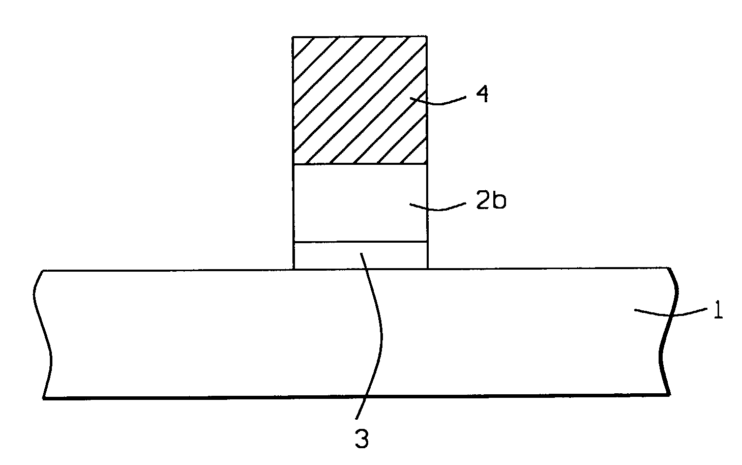
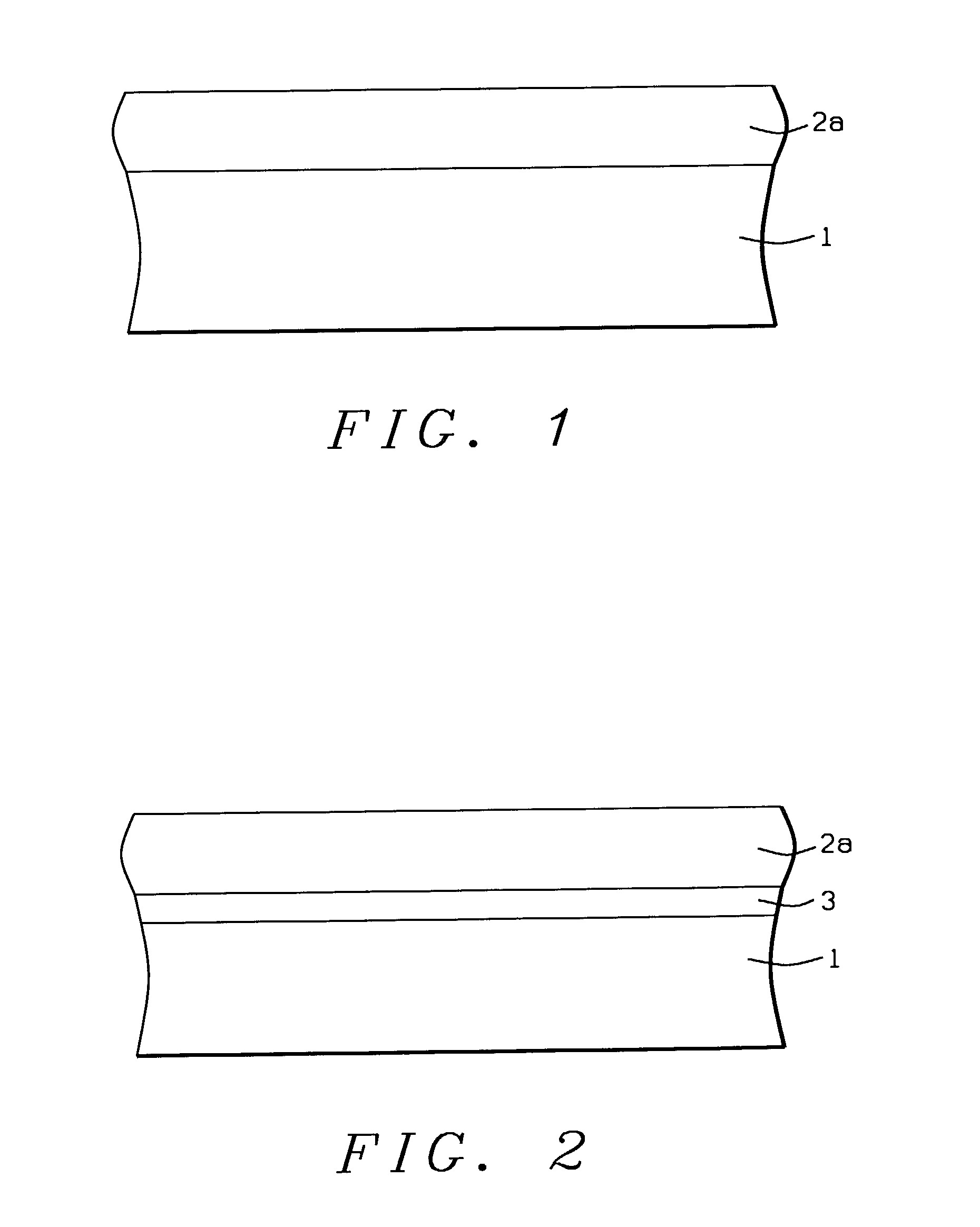
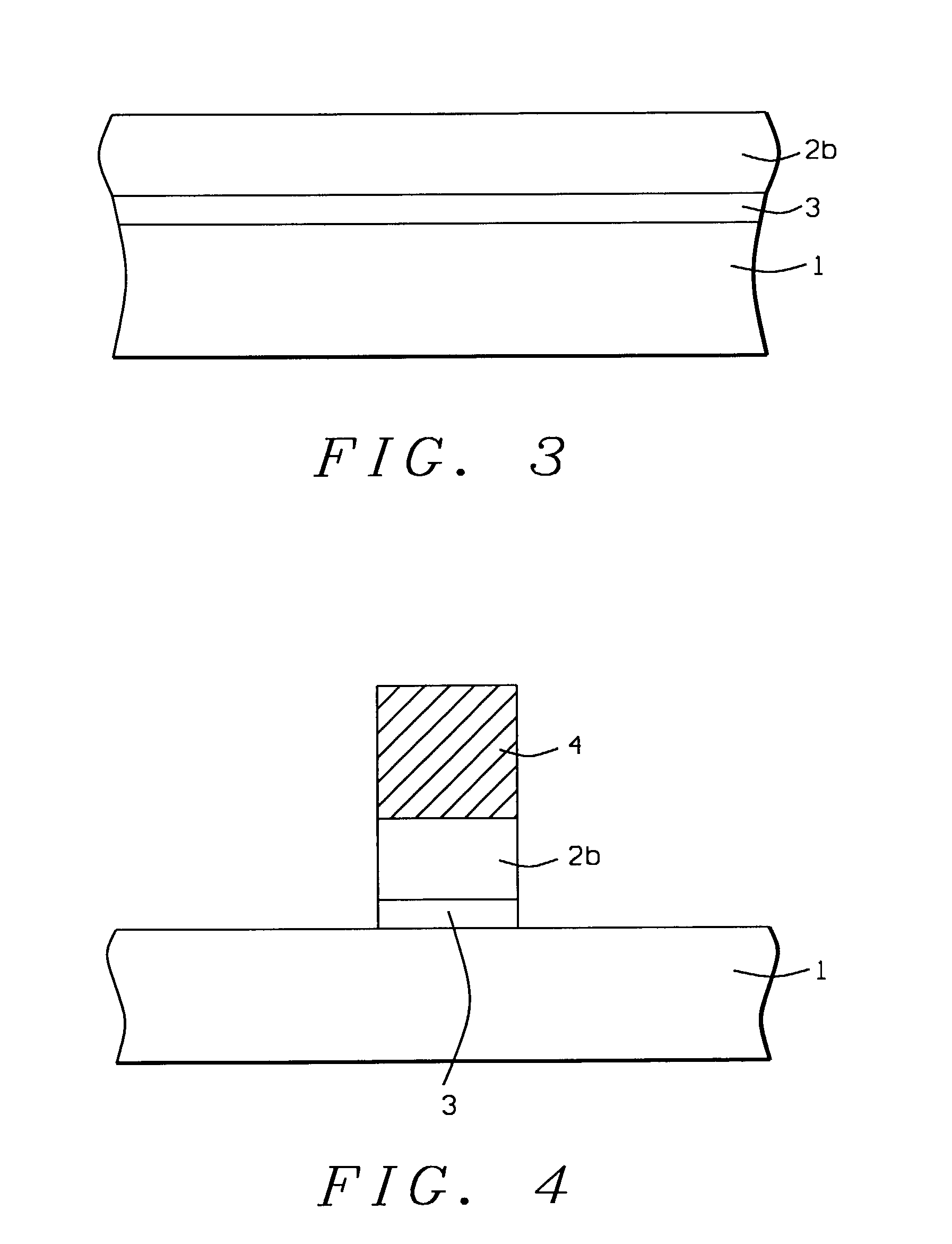
[0012]The method of forming a silicon nitride-silicon dioxide gate dielectric layer via a process sequence allowing reduced gate tunnelling current to be realized, in addition to presenting a barrier to eliminate boron penetration from an overlying boron doped polysilicon gate structure, will now be described in detail. Semiconductor substrate 1, comprised of P type single crystalline silicon, featuring a crystallographic orientation, is used and schematically shown in FIG. 1. Porous, or low density silicon nitride layer 2a, a silicon rich silicon nitride layer, is next deposited on semiconductor substrate 1, at a thickness between about 10 to 30 Angstroms, via low pressure chemical vapor deposition (LPCVD), or via plasma enhanced chemical vapor deposition (PECVD), procedures. The objective is to form a porous, or low density silicon nitride layer which will allow a subsequent thermal oxidation procedure to form a thin silicon dioxide layer on the semiconductor surface, via diffusio...


PUM

PropertyMeasurementUnit
thicknessaaaaaaaaaa
temperatureaaaaaaaaaa
thicknessaaaaaaaaaa

Abstract

A method of forming a silicon nitride-silicon dioxide, composite gate dielectric layer, offering reduced risk of boron penetration from an overlying boron doped polysilicon gate structure, has been developed. A porous, silicon rich silicon nitride layer is first deposited on a semiconductor substrate, allowing a subsequent thermal oxidation procedure to grow a thin silicon dioxide layer on the semiconductor substrate, underlying the porous, silicon rich silicon nitride layer. A two step anneal procedure is then employed with a first step performed in a nitrogen containing ambient to densify the porous, silicon rich silicon nitride layer, while a second step of the anneal procedure, performed in an inert ambient at a high temperature, reduces the foxed charge at the silicon dioxide-semiconductor interface.

Description

BACKGROUND OF THE INVENTION[0001](1) Field of the Invention[0002]The present invention relates to methods used to fabricate semiconductor devices and more specifically to a method used to fabricate a gate dielectric layer offering reduced tunnelling current and improved boron penetration characteristics.[0003](2) Description of Prior Art[0004]Micro-miniaturization, or the ability to fabricate semiconductor devices with sub-micron features, has allowed the performance of sub-micron devices to be increased while the fabrication costs for these same devices have been reduced. The scaling down of semiconductor devices, such as N channel metal oxide semiconductor (NMOS), and P channel (PMOS), elements of complimentary metal oxide semiconductor (CMOS), has included the scaling down of the thickness of the gate insulator layer. The use of thin gate insulator layers have however presenting yield problems not encountered for counterpart devices comprised with thicker gate insulator layers. F...

Claims


Application Information

Patent Timeline
Patent Type & Authority Patents(United States)
IPC IPC(8): H01L21/31H01L21/28H01L21/324H01L21/8238H01L29/51
CPCH01L21/28185H01L29/518H01L21/823842H01L29/513H01L21/324H01L21/28194H01L21/28211
Inventor ANG, CHEW HOELEK, ALANLIN, WENHE
Owner CHARTERED SEMICONDUCTOR MANUFACTURING
Why Eureka
Try Eureka