FeRAM capacitor stack etch

a capacitor and stack etching technology, applied in the field of integrated circuit processing, can solve the problems of metallization not being compatible with a minimum feram cell size, cost disadvantages for embedded memory applications, transistors and other front-end devices, etc., to achieve the effect of minimizing cell size, less sensitive, and cost advantage per bi

Inactive Publication Date: 2006-04-18
TEXAS INSTR INC
View PDF13 Cites 133 Cited by
  • Summary
  • Abstract
  • Description
  • Claims
  • Application Information

AI Technical Summary

Benefits of technology

[0016]The FeRAM process module must therefore be compatible with front-end process flow including the use of W contacts (currently standard in most logic flows) as the bottom contact of the capacitor. The FeRAM thermal budget must also be low enough so that it does not impact the front-end structures such as the low resistance structures (such as tungsten plugs and silicided source / drains and gates) required by most logic devices. In addition, transistors and other front-end devices such as diodes are sensitive to contamination and the FeRAM process module cannot contaminate these devices either directly (diffusion in chip) or indirectly (cross contamination through shared equipment). The FeRAM devices and process module must also be compatible with a standard back end process flow. Therefore the FeRAM process module must have minimum degradation of logic metallization resistance and parasitic capacitance between metal and transistor. In addition, the FeRAM devices must not be degraded by the back end process flow with minimal, if any, modification. This is a significant challenge since ferroelectric capacitors have been shown to be sensitive to hydrogen degradation and most logic back end process flows use hydrogen / deuterium in many of the processes (SiO2, Si3N4, and CVD W deposition, SiO2 via etch, and forming gas anneals).
[0017]Commercial success of FeRAM also requires minimization of embedded memory cost. Total memory cost is primarily dependent on cell size, periphery ratio size, impact of yield, and additional process costs associated with memory. In order to have a cost advantage per bit compared to standard embedded memories such as embedded DRAM and Flash it is necessary to have cell sizes that are not much larger than these competing technologies. Some of the methods discussed in this patent to minimize cell size is to make the process flow less sensitive to lithography misalignment, have the capacitor directly over the contact, and using a single mask for the capacitor stack etch.
[0018]In accordance with one aspect of the present invention, a method of forming an FeRAM capacitor is provided in which the etching of the ferroelectric capacitor stack is greatly improved. The method comprises an etch of the capacitor stack using a patterning hard mask, for example, a TiAlN hard mask. An etch of the PZT ferroelectric layer during the capacitor stack etch comprises a BCl3 etch at a substantially high temperature, for example, about 150° C. or more (e.g., 350° C.). Surprisingly, the BCl3 PZT etch at a relatively high temperature is substantially selective with respect to the overlying patterned hard mask, thereby providing a quality etched PZT film without substantial hard mask erosion, thereby resulting in good critical dimension control of the capacitor stack.
[0019]In accordance with another aspect of the present invention, the capacitor stack comprises iridium top and bottom electrode layers, and a PZT ferroelectric layer disposed between the top and bottom electrode layers. A nitride hard mask, for example, TiAlN, is formed and patterned over the capacitor stack layers. A Cl2+O2 or a Cl2+CO etch is employed to pattern the top electrode layer, wherein the oxygen content therein helps provide a substantial etch selectivity with respect to the hard mask. The PZT layer is then etched with a BCl3 etch at a temperature of at least about 150° C. Unexpectedly, the high temperature BCl3 etch provides good selectivity with respect to the hard mask despite the fact that no oxygen is provided during such etch, thereby providing for a high quality etched PZT film without substantial erosion of the hard mask. Accordingly, a minimal capacitor stack critical dimension is maintained. The bottom electrode is then etched in a manner similar to that of the top electrode layer.
[0020]In accordance with another aspect of the present invention, a capacitor stack etch is disclosed in which a sidewall profile of the PZT ferroelectric layer is made non-vertical. Use of a sloped or non-vertical PZT sidewall profile is not obvious because typically vertical or closely vertical sidewalls are desired to minimize the critical dimension of the capacitor. The PZT sidewall profile is made non-vertical (e.g., less than about 88 degrees) in order to facilitate ion impingement thereon during the subsequent etch of the bottom electrode layer. The ion impingement (e.g., chlorine ions) on the sloped PZT sidewall during the bottom electrode layer etch ensures that re-deposition of conductive bottom electrode material onto the PZT sidewall does not occur by having the removal rate thereof be greater than the deposition rate due to re-sputtering. Accordingly, after the bottom electrode etch, no bottom electrode material resides on the PZT sloped sidewall, thereby preventing leakage or a shorting out of the FeRAM capacitor.
[0021]In accordance with still another aspect of the present invention, a capacitor stack etch having a sloped PZT sidewall profile comprises etching the PZT layer with a fluorine+Cl2+oxidizer etch chemistry at a low temperature, for example, about 60° C. The low temperature causes the sidewall profile of the PZT to not be vertical (a non-anisotropic etch). In addition, the low PZT etch temperature surprisingly eliminates gaps or voids in the PZT ferroelectric layer that occurred with fluorine containing etch chemistries at high temperatures. In one particular example, the PZT etch comprises a CHF3+Cl2+O2+N2 at a temperature of about 60° C., resulting in a PZT sidewall profile of less than about 88 degrees. A PZT sidewall angle of less than 88 degrees is sufficient to ensure no net deposition of conductive material thereon during the subsequent patterning of the underlying bottom electrode layer.

Problems solved by technology

One disadvantage of the approach is that either Metal-1 or a local interconnect must be compatible with FeRAM process temperature (W for example) or the FeRAM process temperature must be lowered to be compatible with standard metallization (Al˜450 C, Cu-Low-K˜400 C).
This location has some advantages for commodity memory purposes, but has cost disadvantages for embedded memory applications.
This solution has the drawback of requiring FeRAM process temperatures compatible with standard metallization plus wiring of the FeRAM capacitor to transistor and other needs of metallization are not compatible with a minimum FeRAM cell size.
In addition, transistors and other front-end devices such as diodes are sensitive to contamination and the FeRAM process module cannot contaminate these devices either directly (diffusion in chip) or indirectly (cross contamination through shared equipment).
This is a significant challenge since ferroelectric capacitors have been shown to be sensitive to hydrogen degradation and most logic back end process flows use hydrogen / deuterium in many of the processes (SiO2, Si3N4, and CVD W deposition, SiO2 via etch, and forming gas anneals).

Method used


Image

  • FeRAM capacitor stack etch
  • FeRAM capacitor stack etch
  • FeRAM capacitor stack etch

Examples


Embodiment Construction

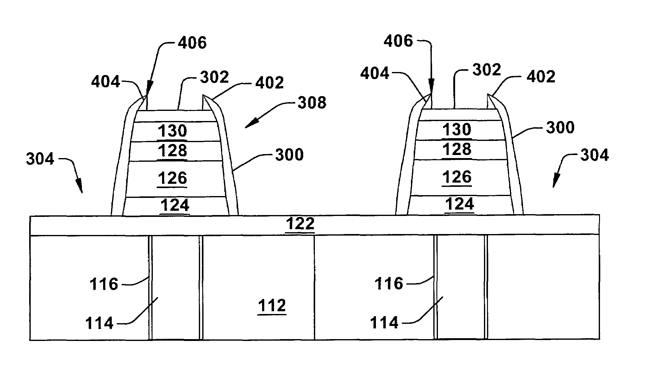
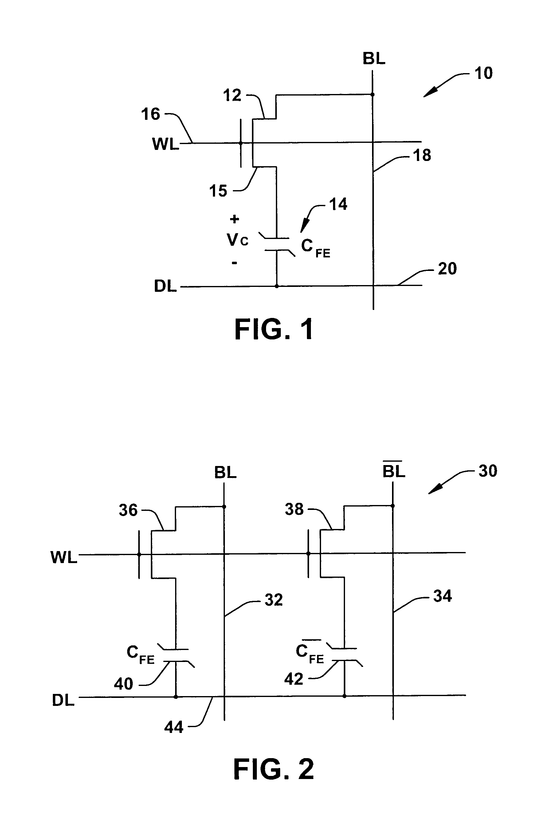
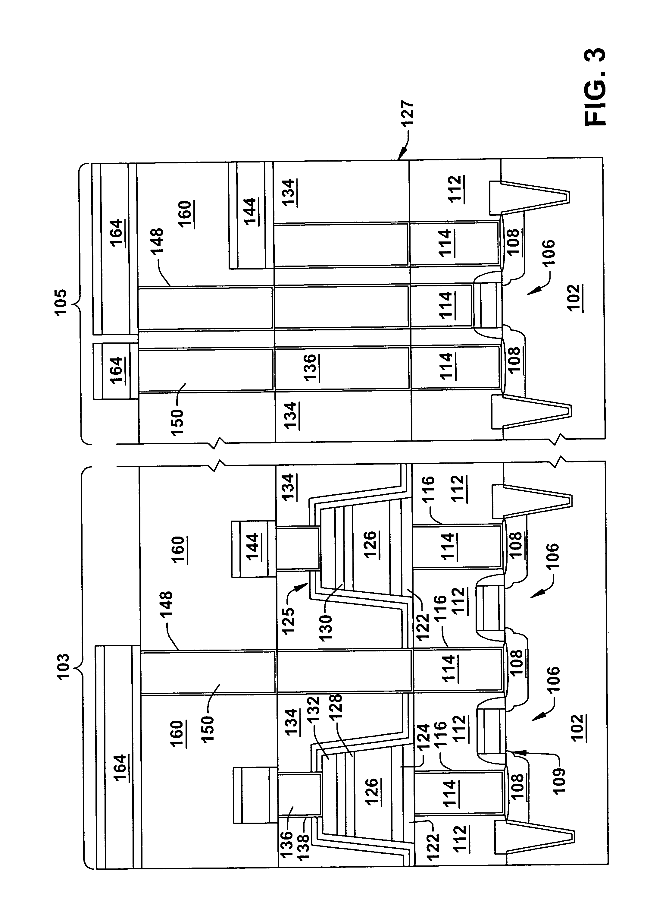
[0037]The present invention will now be described with respect to the accompanying drawings in which like numbered elements represent like parts. While the following description of the instant invention revolves around the integration of the FeRAM devices with logic devices and other devices which can be found on a digital signal processor, microprocessor, smart card, microcomputer, microcontroller or system on a chip, the instant invention can be used to fabricate stand-alone FeRAM devices or FeRAM devices integrated into a semiconductor chip which has many other device types. In particular, the improved performance of the FeRAM device of the instant invention compared to standard semiconductor memories appears to make FeRAM the memory of choice for any handheld device which requires low power and large degree of device integration.

[0038]The figures provided herewith and the accompanying description of the figures are provided for illustrative purposes. One of ordinary skill in the...


PUM


Abstract

The present invention is directed to a method of forming an FeRAM integrated circuit, which includes performing a capacitor stack etch to define the FeRAM capacitor. The method comprises etching a PZT ferroelectric layer with a high temperature BCl3 etch which provides substantial selectivity with respect to the hard mask. Alternatively, the PZT ferroelectric layer is etch using a low temperature fluorine component etch chemistry such as CHF3 to provide a non-vertical PZT sidewall profile. Such a profile prevents conductive material associated with a subsequent bottom electrode layer etch from depositing on the PZT sidewall, thereby preventing leakage or a “shorting out” of the resulting FeRAM capacitor.

Description

RELATED APPLICATIONS[0001]This application is a divisional of Ser. No. 10 / 282,621 filed Oct. 29, 2002 abandoned, which is entitled “FeRAM Capacitor Stack Etch” which also claims priority to Ser. No. 60 / 353,535 filed Jan. 31, 2002, which is entitled “FeRAM Capacitor Stack Etch”.FIELD OF THE INVENTION[0002]The present invention relates generally to the field of integrated circuit processing, and more particularly relates to an FeRAM structure and a method of manufacture thereof having a capacitor stack etch which effectively etches the ferroelectric dielectric layer without degradation thereof.BACKGROUND OF THE INVENTION[0003]Several trends exist, today, in the semiconductor device fabrication industry and the electronics industry. Devices are continuously getting smaller and smaller and requiring less and less power. A reason for this is that more personal devices are being fabricated which are very small and portable, thereby relying on a small battery as its supply source. For exam...

Claims


Application Information

Patent Timeline
Patent Type & Authority Patents(United States)
IPC IPC(8): H01L21/00H01L21/8242H01L21/3065H01L21/02H01L21/311H01L21/316H01L21/3213H01L21/8246H01L27/105H01L27/115
CPCH01L21/31122H01L21/31691H01L28/55H01L27/11502H01L27/11507H01L21/32139H01L21/02197H10B53/30H10B53/00
Inventor CELII, FRANCIS G.SUMMERFELT, SCOTT R.THAKRE, MAHESH
Owner TEXAS INSTR INC
Why Eureka
Try Eureka