Tape stiffener, semiconductor device component assemblies including same, and stereolithographic methods for fabricating same

a technology of tape stiffener and semiconductor device, which is applied in the field of tape structure, can solve the problems of bending of such tapes, torsional flexion and bending of tapes, and difficulty in holding tapes in place to make desired connections,

Inactive Publication Date: 2006-04-18
MICRON TECH INC
View PDF34 Cites 5 Cited by
  • Summary
  • Abstract
  • Description
  • Claims
  • Application Information

AI Technical Summary

Problems solved by technology

Since these tapes are usually flexible, it is sometimes difficult to hold the tape in place to make the desired connections with a semiconductor device component.
This is particularly true in TBGA packages, where torsional flexion and bending of the tape are undesirable during bonding of the contact pads of the tape to the bond pads of a semiconductor die.
Bending of such tapes is also somewhat undesirable in TAB operations where a row of bond pads, other contact pads, or leads of a semiconductor device component are being bonded to an adjacent row of contact pads on the tape.
While conventional metal stiffeners provide support to a tape to be used in a TBGA package, they only support the tape for purposes of connection to the semiconductor die and portions of the tape that extend laterally beyond the periphery of the semiconductor die.
Thus, other portions of the tape that are prone to flexing or damage during assembly of the tape with a semiconductor die, such as the sprocket or indexing holes of a strip of TBGA tapes, are not reinforced.
However, to the inventor's knowledge, stereolithography has yet to be applied to mass production of articles in volumes of thousands or millions, or employed to produce, augment or enhance products including other, pre-existing components in large quantities, where minute component sizes are involved, and where extremely high resolution and a high degree of reproducibility of results are required.
Furthermore, conventional stereolithography apparatus and methods fail to address the difficulties of precisely locating and orienting a number of pre-existing components for stereolithographic application of material thereto without the use of mechanical alignment techniques or to otherwise assuring precise, repeatable placement of components.

Method used


Image

  • Tape stiffener, semiconductor device component assemblies including same, and stereolithographic methods for fabricating same
  • Tape stiffener, semiconductor device component assemblies including same, and stereolithographic methods for fabricating same
  • Tape stiffener, semiconductor device component assemblies including same, and stereolithographic methods for fabricating same

Examples


Embodiment Construction

Stiffeners

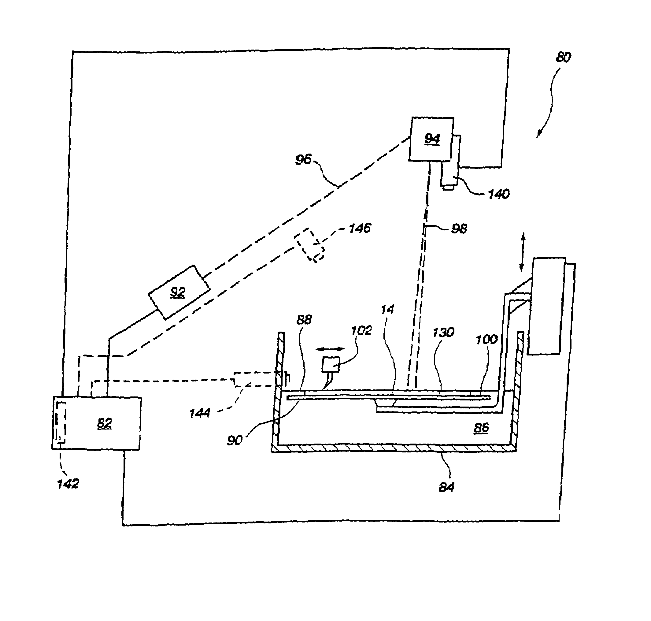
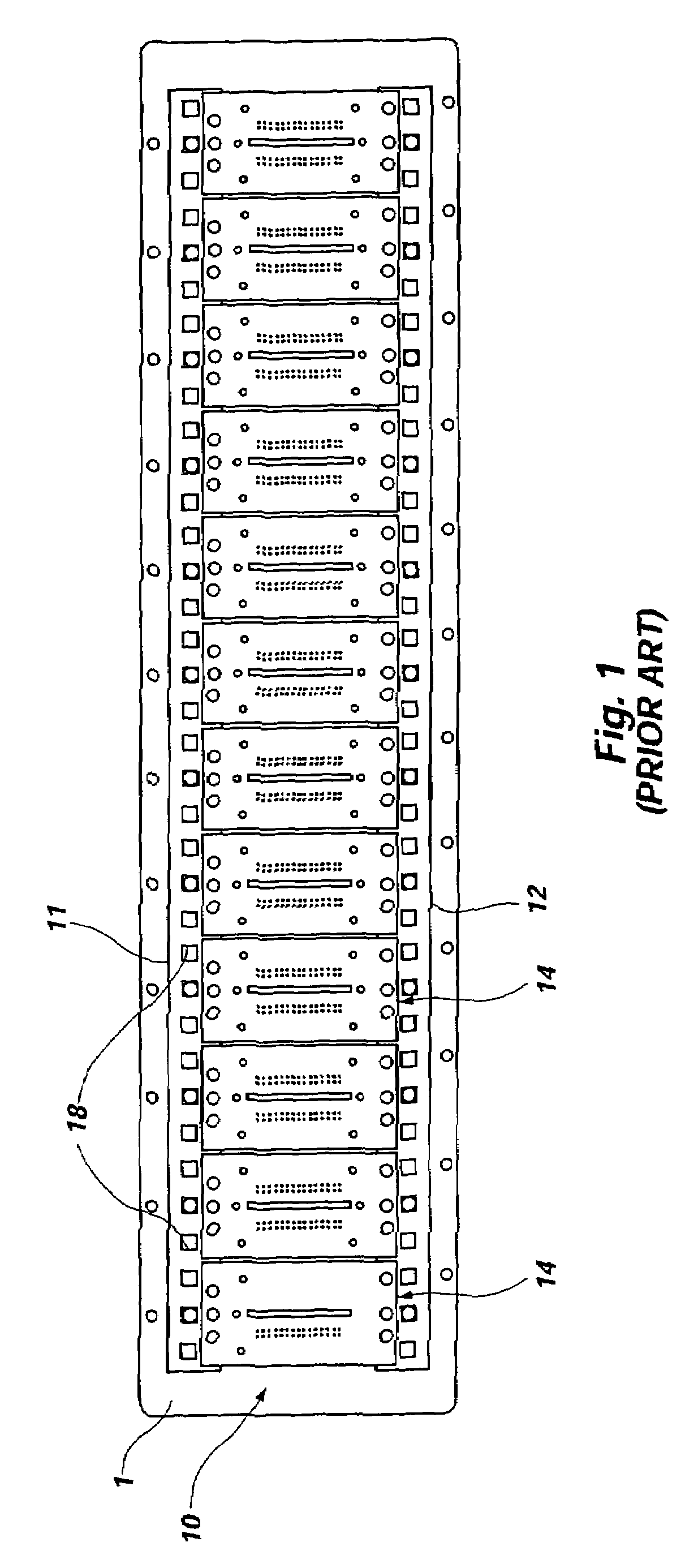
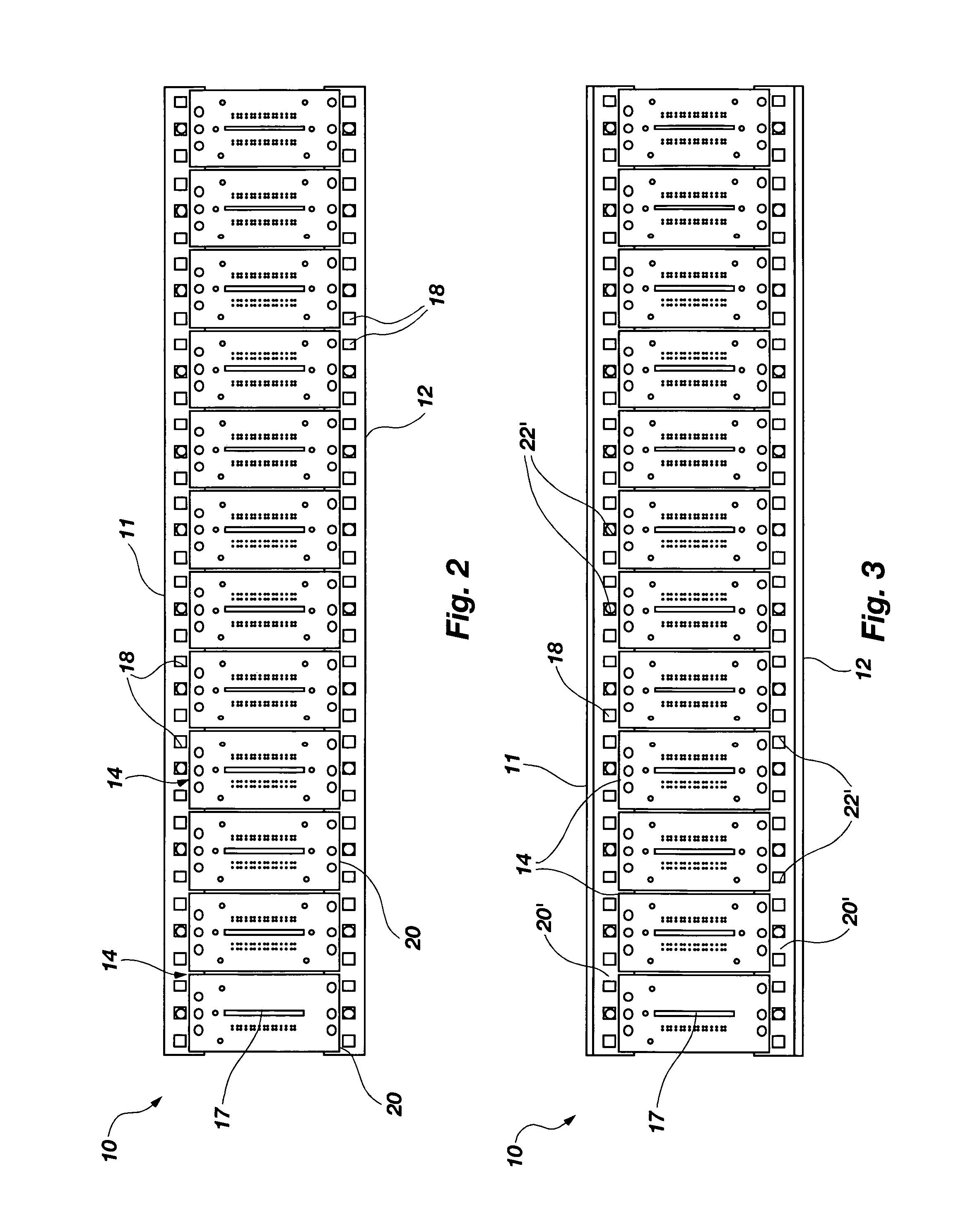
[0041]With reference to FIG. 2, a strip 10 of tapes 14 for use in TBGA packages or other TAB applications is illustrated. Each tape 14, which may be a TBGA tape or TAB tape of known configuration, includes electrically conductive circuit traces 15 (see, e.g., FIG. 6) thereon, some of which lead to contact pads positioned on the opposite side of tape 14. Tape 14 also includes apertures 17 to facilitate the formation of electrical connections therethrough. Sprocket or indexing holes 18 are located near the top and bottom edges 11, 12 of strip 10 and are consistently spaced apart from one another along the top and bottom edges 11, 12 of strip 10 so as to facilitate mechanical indexing of strip 10.

[0042]A stiffener 20 is secured to each tape 14. Each stiffener 20 shown in FIG. 2 extends adjacent the substantial periphery of the corresponding tape 14. Stiffeners 20 are preferably formed from a rigid dielectric material, such as a photocurable polymer, or photopolymer, to preven...


PUM

PropertyMeasurementUnit
thicknessaaaaaaaaaa
thickaaaaaaaaaa
thicknessaaaaaaaaaa

Abstract

Stiffeners for tapes, films, or other connective structures, which are configured to be secured to a semiconductor device component, such as a semiconductor die or substrate, by tape-automated bonding processes, are fabricated by stereolithographic processes and may include one or two or more layers. The stiffeners are configured to prevent torsional flexion or bending of the connective structure to which they are to be secured. The stiffeners may reinforce sprocket or indexing holes in connective structures. The stiffeners may include apertures through which intermediate conductive elements or other structures secured to the connective structure may be exposed or protrude. The stereolithographic method for fabricating stiffeners may include use of a machine vision system that recognizes the position and orientation of one or more connective structures on which at least an element of each of the stiffeners is to be fabricated so that the application of material thereto may be controlled.

Description

CROSS-REFERENCE TO RELATED APPLICATIONS[0001]This application is a continuation of application Ser. No. 10 / 436,939, filed May 13, 2003, now U.S. Pat. No. 6,746,899, issued Jun. 8, 2004, which is a continuation of application Ser. No. 09 / 903,241, filed Jul. 11, 2001, now U.S. Pat. No. 6,562,661, issued May 13, 2003, which is a divisional of application Ser. No. 09 / 512,203, filed Feb. 24, 2000, now U.S. Pat. No. 6,740,962, issued May 25, 2004.BACKGROUND OF THE INVENTION[0002]1. Field of the Invention[0003]The present invention relates generally to tape structures that are used in assemblies of semiconductor device components, such as the flexible dielectric tapes that are used in tape automated bonding (TAB) and tape ball grid array (TBGA) packages. Particularly, the tapes of the present invention have stiffeners, or support structures, thereon. More specifically, the present invention relates to tapes with stereolithographically fabricated stiffeners. The present invention also relat...

Claims


Application Information

Patent Timeline
Patent Type & Authority Patents(United States)
IPC IPC(8): H01L21/44H01L21/48H01L21/50G03F7/20H01L23/498H05K1/00H05K3/00
CPCG03F7/70416H01L21/67132H01L23/49833H01L23/4985H01L24/86H05K3/0097H01L21/4839H01L2924/014H01L23/3128H01L2224/4824H01L2924/01013H01L2924/01029H01L2924/01082H01L2924/15311H05K1/0393H05K3/0023H05K2201/09909H05K2201/2009H05K2203/1545H01L24/48H01L2924/01005H01L2924/01033H01L2924/351H01L2924/12042H01L2224/05624H01L2224/45144H01L2224/85424H01L2924/00014Y02P80/30H01L2924/181H01L24/50B33Y80/00B33Y10/00B33Y30/00
Inventor GRIGG, FORD B.
Owner MICRON TECH INC
Why Eureka
Try Eureka