

Semiconductor device and method of manufacturing the same
- Summary
- Abstract
- Description
- Claims
- Application Information
AI Technical Summary
Benefits of technology
Problems solved by technology
Method used
Image

Examples
first embodiment
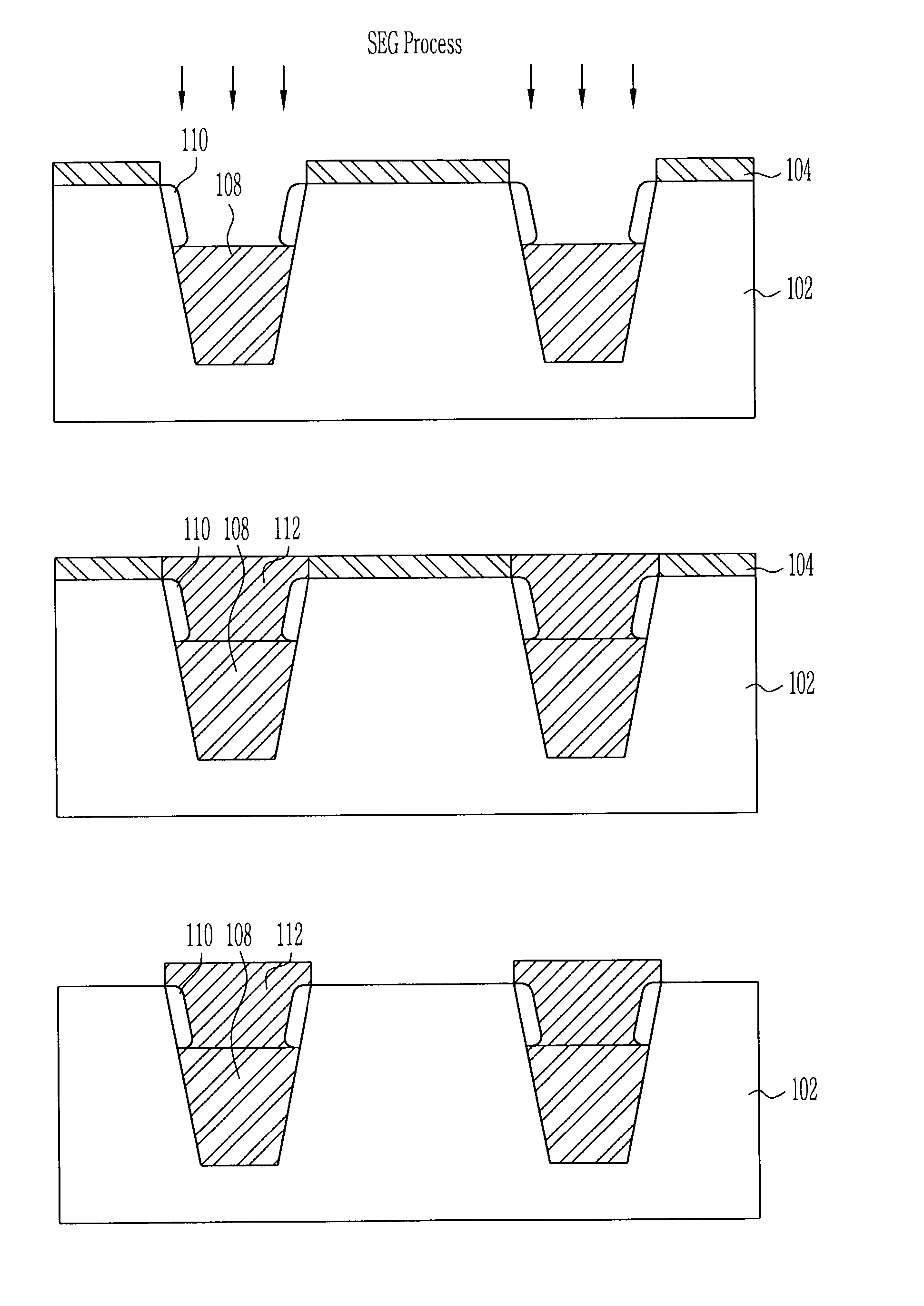
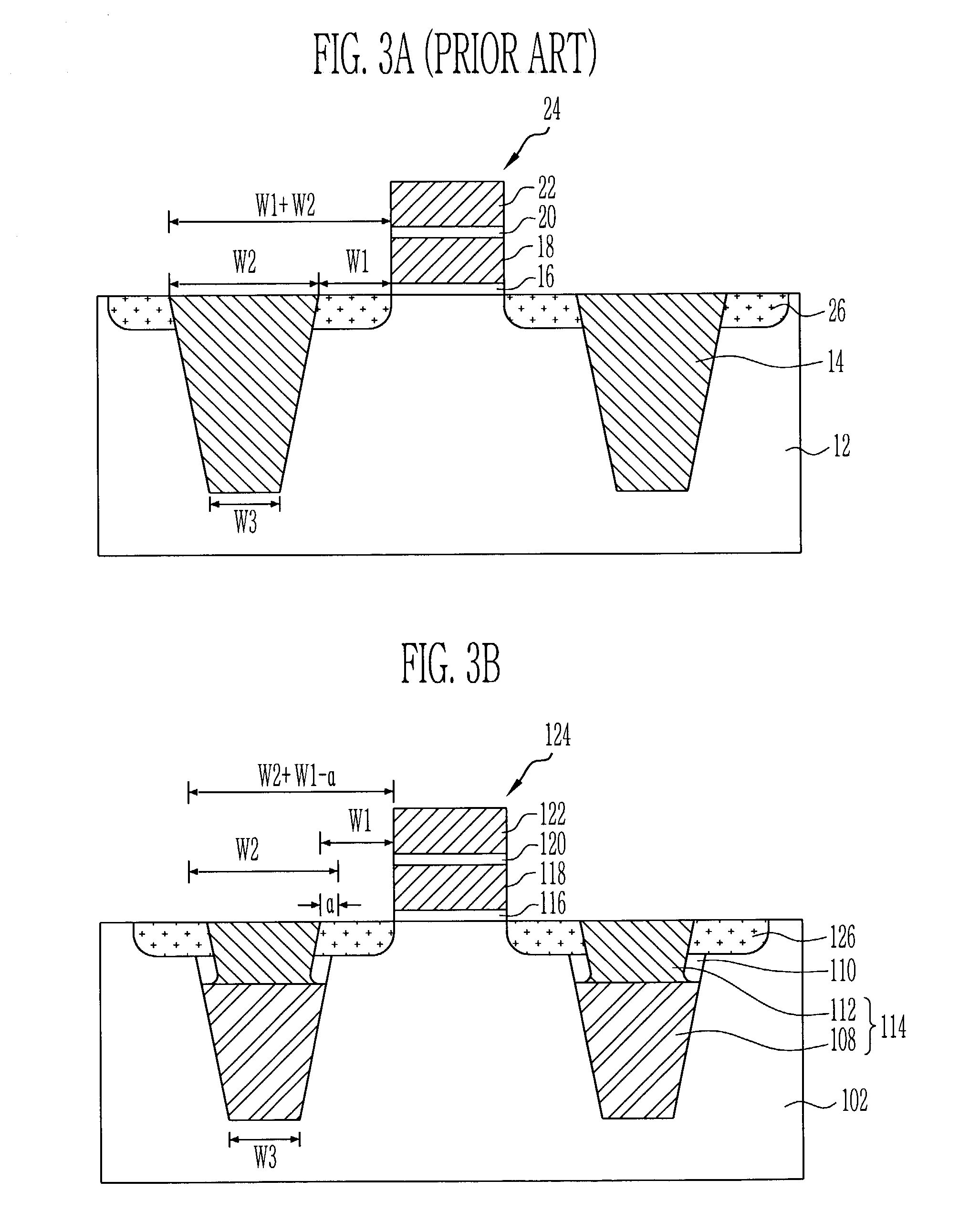
[0023]FIG. 1 is a cross sectional view of a semiconductor device according to the present invention.
[0024]Referring now to FIG. 1, the semiconductor device according to the first embodiment of the present invention comprises a plurality of impurity diffusion layers 126 serving as source / drain, and a plurality of gates 124. The semiconductor device further comprises a device isolation film 114 for electrically isolating single devices (for example, unit cell, transistor) consisting of the impurity diffusion layer 126 and the gates 124.
[0025]The impurity diffusion layer 126 is formed in the semiconductor substrate 102 at both sides of the gates 124. One end of the impurity diffusion layer 126 adjoins the gates 124. The other end of the impurity diffusion layer 126 is extended to a silicon growth layer 110 formed in a device isolation region where the device isolation film 114 is formed. At this time, for convenience of explanation, it is shown that the impurity diffusion layer 126 is ...
second embodiment
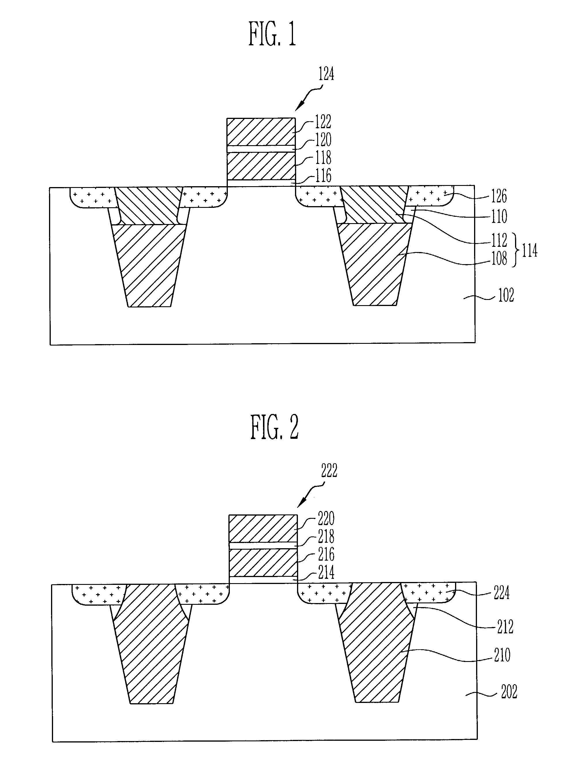
[0032]FIG. 2 is a cross sectional view of a semiconductor device according to the present invention.
[0033]In the second embodiment of the present invention, the number of the process can be reduced compared to those in the first embodiment, by applying the technical idea of the first embodiment of the present invention to a moat portion of the sidewall of the trench generating after the device isolation film is formed.
[0034]Referring now to FIG. 2, the semiconductor device according to the second embodiment comprises a plurality of impurity diffusion layers 224, a plurality of gates 222, an impurity diffusion layer 224, and a device isolation film 210 of a trench structure that is formed using the STI process in order to electrically isolate the single devices consisting of the gates 222, as in the first embodiment. The gate 222 comprises a gate insulating film 214, a floating gate 216, a dielectric film 218 and a control gate 220.
[0035]It was described that the device isolation fil...
PUM
 Abstract
Description
Claims
Application Information