

Optical waveguide, forming material and making method
a technology of optical waveguides and forming materials, applied in the direction of photomechanical instruments, photomechanical equipment, originals for photomechanical treatment, etc., to achieve the effects of high sensitivity and resolution, convenient processing, and satisfactory patterning performan
- Summary
- Abstract
- Description
- Claims
- Application Information
AI Technical Summary
Benefits of technology
Problems solved by technology
Method used
Image

Examples
example 1
[0040]As an optical waveguide clad-forming material, 0.15 mol of 2-(3,4-epoxycyclohexylethyl)trimethoxysilane (1) and 0.15 mol of phenyltrimethoxysilane (2) were added to methanol solvent. Separately, as a core-forming material, 0.06 mol of 2-(3,4-epoxycyclohexylethyl)trimethoxysilane (1) and 0.24 mol of phenyltrimethoxysilane (2) were added to methanol solvent. To the respective solutions, with stirring, a mixture of deionized water and conc. hydrochloric acid as an acid catalyst was added dropwise to effect hydrolytic reaction at 25° C. Next, each reaction mixture was heated under reflux in an oil bath at 100° C. for at least one hour to effect polycondensation reaction. Polycondensation reaction was continued for a further 2 hours in the oil bath at 100° C. while the solvent and alcohol by-products formed were being distilled off. The thus obtained hydrolytic condensate was washed with water and dissolved in tetrahydrofuran. The solution was passed through a filter with a pore di...
example 2
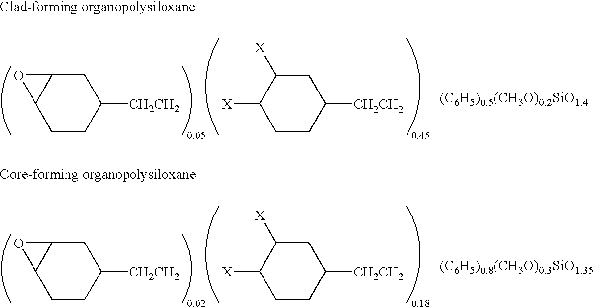
[0046]The procedure of Example 1 was repeated except that 0.24 mol of 2-(3,4-epoxycyclohexylethyl)trimethoxysilane (1) and 0.06 mol of phenyltrimethoxysilane (2) were used as the optical waveguide clad-forming material, and 0.15 mol of 2-(3,4-epoxycyclohexylethyl)trimethoxysilane (1) and 0.15 mol of phenyltrimethoxysilane (2) were used as the core-forming material. There were obtained alkali-soluble organopolysiloxanes of the following average compositional formulae.
[0047]
Note that two X's are —OH and —Cl, —OH and —OH, or —OH and —OCH3.
[0048]On GPC analysis, the clad-forming polysiloxane (C) had Mw of 3200 and the core-forming polysiloxane (D) had Mw of 2800.
[0049]Using the polysiloxanes, optical waveguide-forming materials (C) and (D) were prepared as in Example 1. After photocuring, the materials (C) and (D) had a refractive index at 850 nm of 1.5106 and 1.5264, respectively.
[0050]Using the polysiloxanes (C) and (D), an optical waveguide of the embedment type was fabricated as in ...
example 3
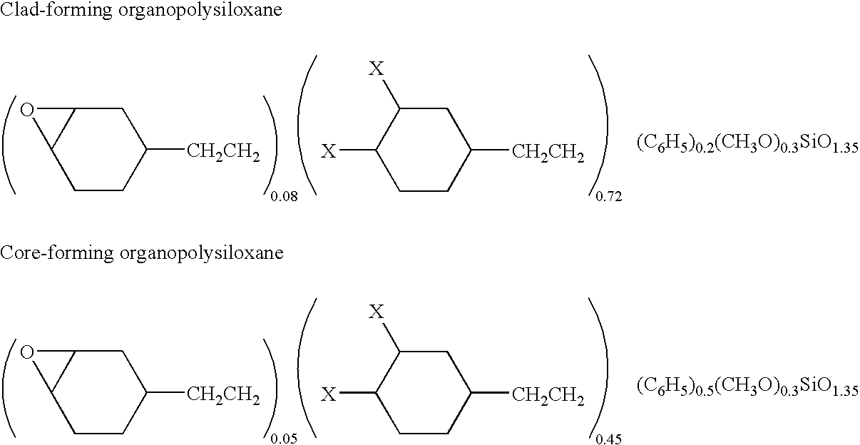
[0051]The procedure of Example 1 was repeated except that 0.30 mol of 2-(3,4-epoxycyclohexylethyl)trimethoxysilane (1) was used as the optical waveguide clad-forming material, and 0.18 mol of 2-(3,4-epoxycyclohexylethyl)trimethoxysilane (1) and 0.12 mol of phenyltrimethoxysilane (2) were used as the core-forming material. There were obtained alkali-soluble organopolysiloxanes of the following average compositional formulae.
[0052]
Note that two X's are —OH and —Cl, —OH and —OH, or —OH and —OCH3.
[0053]On GPC analysis, the clad-forming polysiloxane (E) had Mw of 2500 and the core-forming polysiloxane (F) had Mw of 2700.
[0054]Using the polysiloxanes, optical waveguide-forming materials (E) and (F) were prepared as in Example 1. After photocuring, the materials (E) and (F) had a refractive index at 850 nm of 1.5000 and 1.5180, respectively.
[0055]Using the polysiloxanes (E) and (F), an optical waveguide of the embedment type was fabricated as in Example 1. The optical waveguide was measure...
PUM
| Property | Measurement | Unit |
|---|---|---|
| Electrical resistance | aaaaa | aaaaa |
| Photocurable | aaaaa | aaaaa |
| Solubility (mass) | aaaaa | aaaaa |
Abstract
Description
Claims
Application Information