Semiconductor wiring substrate, semiconductor device, method for testing semiconductor device, and method for mounting semiconductor device

a technology for semiconductor devices and wiring substrates, which is applied in the direction of semiconductor/solid-state device testing/measurement, semiconductor/solid-state device details, instruments, etc., can solve the problems of high cost of system lsis development, difficulty in reducing device manufacturing costs, and above-described conventional system lsis are confronted with problems, so as to facilitate the mounting of components and improve the reliability of the ipos device.

Inactive Publication Date: 2006-04-18
SOCIONEXT INC
View PDF11 Cites 15 Cited by
  • Summary
  • Abstract
  • Description
  • Claims
  • Application Information

AI Technical Summary

Benefits of technology

[0057]This method ensures improved reliability of the

Problems solved by technology

The above-described conventional system LSIs are confronted with problems described below in actually forming devices.
The first problem resides in difficulty in reducing the device manufacturing cost.
This is due to a high cost of development of system LSIs and a limited manufacturing yield.
The second problem resides in a considerable increase in wiring delay.
That is, as regards the wiring delay, the disadvantage of a design by a finer rule prevails over the advantage of the same.
However, if a buffer is provided, another problem arises in that the area occupied by a device and the power consumption of the device are increased.
The third problem resides in difficulty in reducing noise.
If the power supply voltage is reduced, the current is increased and it is difficult to limit the in

Method used


Image

  • Semiconductor wiring substrate, semiconductor device, method for testing semiconductor device, and method for mounting semiconductor device
  • Semiconductor wiring substrate, semiconductor device, method for testing semiconductor device, and method for mounting semiconductor device
  • Semiconductor wiring substrate, semiconductor device, method for testing semiconductor device, and method for mounting semiconductor device

Examples


embodiment 1

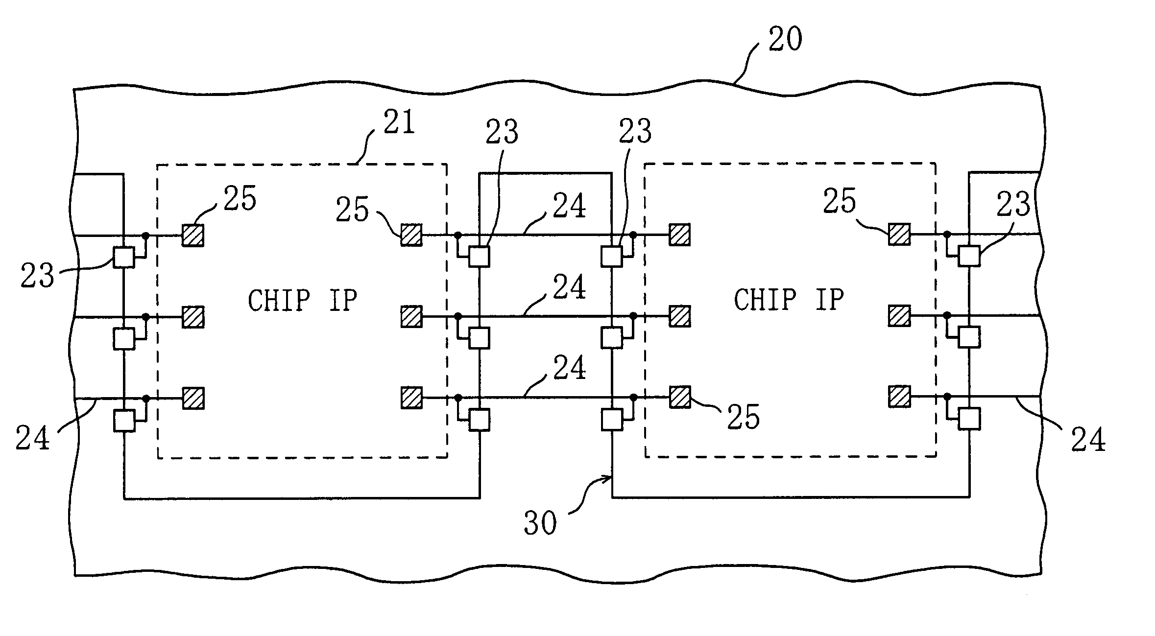
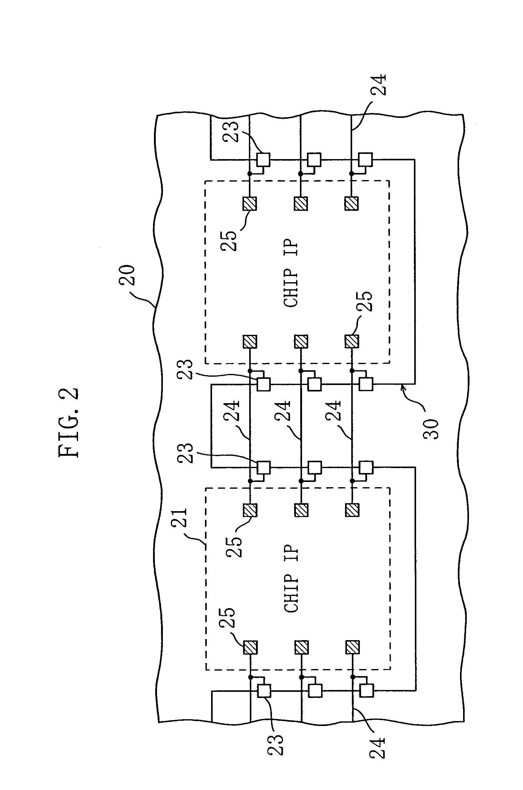
[0094]FIG. 2 is a block diagram showing a circuit configuration on a silicon wiring substrate 20 of a first embodiment of the present invention. On the silicon wiring substrate 20 are formed pads 25 connected to pads of chip IPs by diffusion junction or the like, and pieces of wiring 24 for connection between pairs of the pads 25 (between two chip IPs 21 and 22). This embodiment is characterized in that flip flops 23 are respectively provided in the vicinity of and below end portions of the pieces of wiring 24 located in regions where the chip IPs are mounted (regions indicated by broken lines in the figure). That is, two flip flops 23 are provided at positions close to opposite ends of each piece of wiring 24. The position of each flip flop 23 may be such that the flip flop overlaps the chip IP or does not overlap the chip IP. A scan chain 30 is formed in which the flip flops 23 are successively connected. A boundary scan test can be carried out by using this scan chain 30. For exa...

embodiment 2

[0099]FIG. 4 is a schematic plan view of the structure of an IPOS device in a second embodiment of the present invention. As shown in FIG. 4, the IPOS device of this embodiment has testing pads 31 are placed in a grid pattern on a silicon wiring substrate 20 in regions other than regions RIP where IPs are to be mounted.

[0100]After chip IPs have been mounted on the silicon wiring substrate 20, a scan test or a BIST on the chip IPs can be carried out by using some of the testing pads 31 selected as desired. That is, in this embodiment, with respect to any of various kinds of chip IP mounted in the chip mount regions RIP, a testing method can be selected according to the kind of chip IP and carried out. Different kinds of testing circuit to be used in combination of groups of testing pads may be provided.

[0101]FIG. 5 is a schematic plan view of the structure of testing wiring in this embodiment. As shown in FIG. 5, pieces of testing wiring 32 for connecting testing pads 31 to external ...

embodiment 3

[0104]FIG. 7 is a plan view of an IPOS device in a third embodiment of the present invention. In this embodiment, a multiplicity of chip IPs 43 and a multiplicity of testing pads 41 are placed on a silicon wiring substrate 20. In this embodiment, power supply pads 42 to be used only at the time of testing are provided.

[0105]In this embodiment, additional power supply pads 42 to be used only at the time of testing are provided to achieve an effect described below. In general, a chip IP design for reducing power consumption by allowing only part of chip IPs to operate at a time can be adopted by considering an increased power consumption when all the chip IPs 43 operate simultaneously in actual use. Ordinarily, such a power consumption setting is made to limit the power consumption during operation in actual use. However, at the time of testing without consideration of power consumption, there is a possibility of all the chip IPs 43 on the IPOS device operating at a time. Since the en...


PUM


Abstract

A semiconductor device constructed by mounting a plurality of chip intellectual properties (IPs) on a common semiconductor wiring substrate, a method for testing the device and a method for mounting the chip IPs. A silicon wiring substrate on which chip IPs can be mounted is provided. A circuit for a boundary scan test is formed on the silicon wiring substrate by connecting flip flops. The flip flops are connected to wiring and are arranged to test connections in the wiring. The entire IP On Super-Sub (IPOS) device or each chip IP may be arranged to facilitate a scan test, a built-in self-test (BIST), etc., on the internal circuit of the chip IP.

Description

[0001]This application is a divisonal of Application Ser. No. 10 / 187,269 filed Jul. 2, 2002 now U.S. Pat. No. 6,734,549.BACKGROUND OF THE INVENTION[0002]The concept “system LSI” of a plurality of large-scale integrated circuits (LSIs) on a common substrate has recently been brought in and various methods of designing system LSIs have also been proposed. System LSIs in particular have the advantage of being realized as a wide variety of multifunctional semiconductor devices on an extremely large scale of integration in such a manner that a memory such as a dynamic random access memory (DRAM), a logic LSI, an analog circuit such as a high-frequency circuit, etc., are mounted in one semiconductor device.[0003]As a method for testing each of such LSIs to determine whether the LSI is correctly formed, a built-in self-test (BIST), a scan test and a boundary scan test, for example, are known.[0004]FIG. 24 is a block diagram for explaining a conventional ordinary built-in self-test (BIST). ...

Claims


Application Information

Patent Timeline
IPC IPC(8): G06F17/50G01R31/28H01L23/58G01R31/317G01R31/3183G01R31/3185G06F11/22G11C5/02G11C29/48
CPCG01R31/318538G11C5/025G11C29/48G01R31/318558G01R31/318505G11C2029/3202H01L23/12G11C5/02G01R31/28G06F30/00
Inventor TAKEOKA, SADAMIOHTA, MITSUYASUICHIKAWA, OSAMUYOSHIMURA, MASAYOSHI
Owner SOCIONEXT INC
Why Eureka
Try Eureka