
Circuits to achieve high data rate writing on thin film transducer

a technology of thin film transducer and data rate, applied in the direction of data recording, magnetic recording, instruments, etc., can solve the problem of constant power dissipation, achieve high-speed data transfer, reduce transient voltage and current on supply, and reduce signal reflection

Inactive Publication Date: 2006-04-25
TEXAS INSTR INC
View PDF6 Cites 17 Cited by
  • Summary
  • Abstract
  • Description
  • Claims
  • Application Information

AI Technical Summary

Benefits of technology

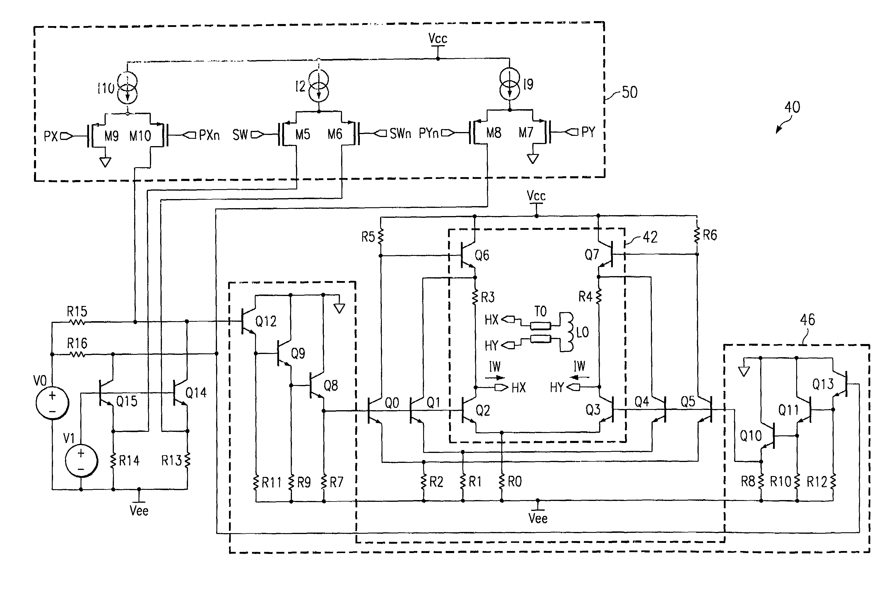
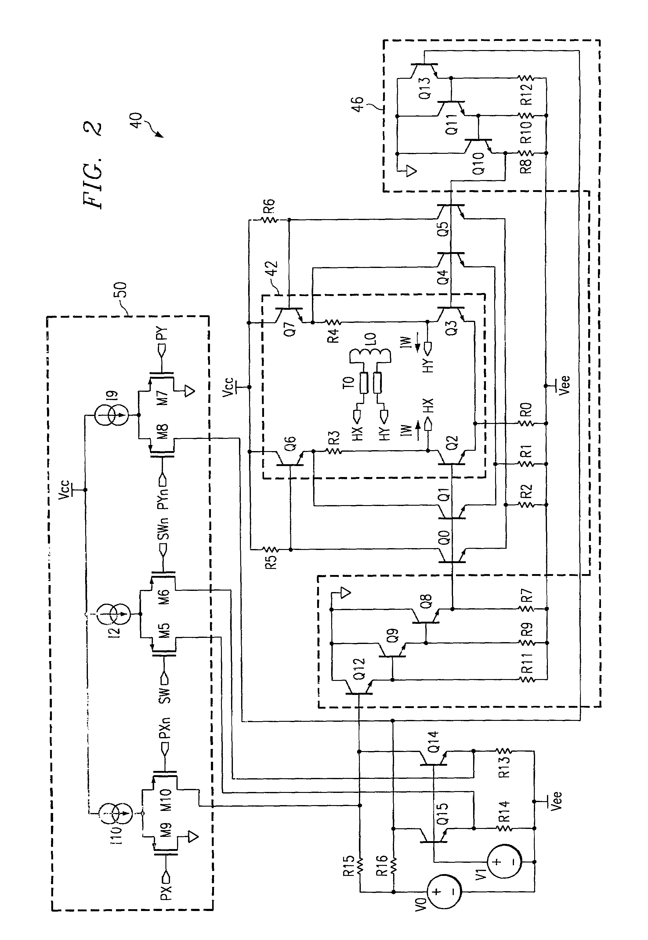
[0006]The present invention achieves technical advantages by using ECL level logic throughout the write data path to achieve high speed data transfer. It also helps reduce transient voltage and current on supplies. The present invention uses NPN transistors and PMOS transistors switching in current mode for critical data switching path. Moreover, internal resistors of an H-switch are matched to the differential impedance of the flex cable interconnection to reduce the signal reflections, which affect the data integrity at high data rate. The present invention uses several emitter-follower stages to build up pre-drivers for the high current H-switch driver and to increase drive current slew rate.
[0007]ECL logic from 250 mV to 2V differential is a better way to transfer high speed data. In addition, the power dissipation is constant when using ECL logic, as compared to the power consumption of CMOS logic which increases with frequency. The advantagous use of PMOS current mode boost circuitry provides a fast slew rate current and large voltage swing at the preamplifier's outputs. Thus, high write data rates can be achieved without the need of expensive vertical PNPs (typically, five layers must be added to have the vertical PNPs). The present circuit provides a simple way to achieve write current accuracy.

Problems solved by technology

In addition, the power dissipation is constant when using ECL logic, as compared to the power consumption of CMOS logic which increases with frequency.

Method used


Image

  • Circuits to achieve high data rate writing on thin film transducer
  • Circuits to achieve high data rate writing on thin film transducer
  • Circuits to achieve high data rate writing on thin film transducer

Examples


Embodiment Construction

[0012]The present invention implements an H-switch high current writer. However, the differences and advantages are the technique to provide ECL-level signals to the inputs of the H-switch rather than using CMOS logic.

[0013]FIG. 2 shows the new write driver 40 including a pulsing circuit 50 and ECL buffers 46. An H-switch 42 write driver consists of transistors Q0–Q7 and resistors R0–R6. The operation of this H-switch 42 is described in copending patent application Attorney's Docket Number TI-31786 entitled “Method to Increase Voltage Swing and Reduce Rise Time of a H Current Switch.” the teachings of which are incorporated herein by reference.

[0014]The ECL pre-driver 46 advantageously includes emitter-follower transistors Q8–Q13 and resistors R8–R12. Three stages of emitter-follower buffer are used to build enough current and voltage drive capability since the output write current Iw provided to the head L0 is typically 60 mA (steady state) and 150 mA (transient / overshoot).

[0015]Th...


PUM


Abstract

The present invention covers circuits to achieve high data rate writing.

Description

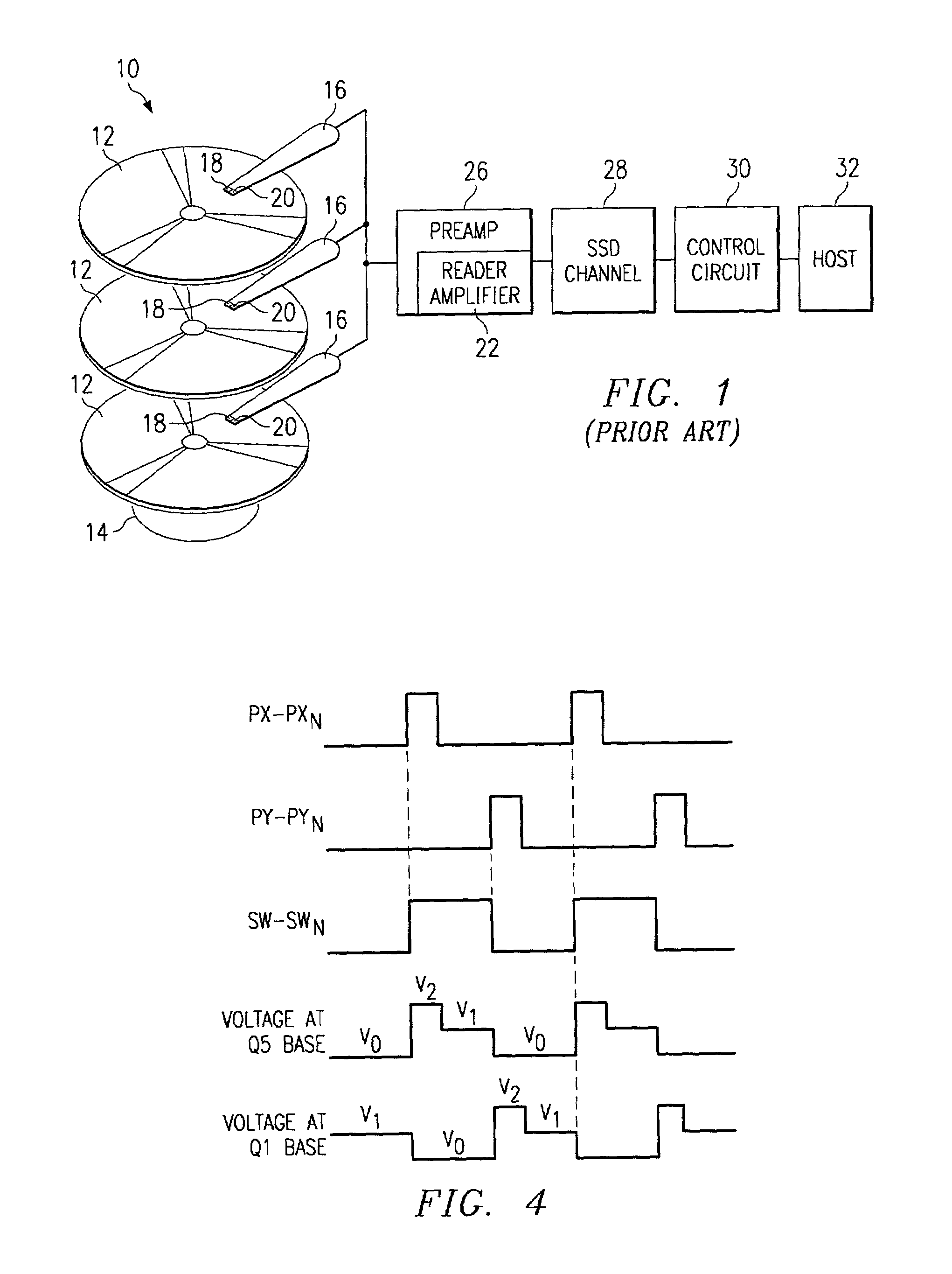
FIELD OF THE INVENTION[0001]The present invention is generally related to the field of mass media information storage devices, and more particularly to a drive circuit and method for increasing the write speed of a write driver.BACKGROUND OF THE INVENTION[0002]Hard disk drives are mass storage devices that include a magnetic storage media, e.g. rotating disks or platters, a spindle motor, read / write heads, an actuator, a pre-amplifier, a read channel, a write channel, a servo circuit, and control circuitry to control the operation of hard disk drive and to properly interface the hard disk drive to a host system or bus. FIG. 1 shows an example of a prior art disk drive mass storage system 10. Disk drive system 10 interfaces with and exchanges data with a host 32 during read and write operations. Disk drive system 10 includes a number of rotating platters 12 mounted on a base 14. The platters 12 are used to store data that is represented as magnetic transitions on the magnetic platter...

Claims


Application Information

Patent Timeline
IPC IPC(8): G11B5/09G11B5/02G11B5/00G11B5/012G11B5/035
CPCG11B5/02G11B5/022G11B5/012G11B2005/0013G11B5/035G11B5/09
Inventor BARNETT, RAYMOND ELIJAHVAN NGO, TUANSORENSON, SCOTT GARY
Owner TEXAS INSTR INC
Learn More