Integrated demultiplexer/photoreceiver for optical networks and method of controlling transparency of optical signal transmission layer

a technology of optical signal transmission layer and optical network, applied in the field of semiconductor devices, can solve the problems of difficult optical alignment, limited number of optical channels, high manufacturing cost, etc., and achieve the effect of simplifying design, improving optical alignment conditions, and reducing cos

Inactive Publication Date: 2006-04-25
XONPHU LINE LIMITED LIABILITY
View PDF3 Cites 0 Cited by
  • Summary
  • Abstract
  • Description
  • Claims
  • Application Information

AI Technical Summary

Benefits of technology

[0008]An integrated demultiplexer / photoreceiver (IDP) for optical networks and optical interconnection devices has a common substrate which supports three sequentially arranged basic components: a waveguide grating router, an array of photodetectors, and an array of heterojunction transistors. All layers of all three components are grown together in a common epitaxial process, and then each of the components is individually patterned in accordance with its function. Such structure of IDP makes it possible to reduce the cost, simplify the design, improve conditions for optical alignment, and reduce optical losses. In accordance with one embodiment of the invention, transparency of the optical signal transmission layer of the WGR is controlled by selectively doping the layers of the multiple-layer waveguide structure, while in another embodiment such control is achieved by utilizing electrical bias and optical pumping from an external light pumping source operating on a predetermined wavelength. The invention also provides a method for controlling transparency of the layer that transmits optical signals through the waveguide units in optoelectronic devices, such as an integrated demultiplexer / photoreceiver for optical network, by utilizing optical pumping and electrical bias.OBJECTS OF THE INVENTION
[0009]It is an object of the present invention to provide an integrated demultiplexer / photoreceiver for optical networks and optical interconnection devices which is simple in construction, inexpensive and simple to manufacture, can be produced in a single manufacturing process for all basic components, characterized by reduced optical losses, and facilitates optical alignment. The invention also provides a method for manufacturing the aforementioned demultiplexer / photoreceiver, which is simple, inexpensive, and may require a fewer number of steps than known methods. Another object is to provide control of transparency in the optical signal transmission layer of WGR by selectively doping the multiple-layer structure of the WGR. Still another object is to provide control of transparency in the optical signal transmission layers of devices, such as WGR, by utilizing electrical bias and optical pumping with the use of a light pumping source operating on a predetermined wavelength.

Problems solved by technology

A disadvantage of a photoreceiving unit assembled from three prefabricated devices is that it is large in size, expensive to manufacture, requires assembling operation, involves optical losses, makes it difficult to provide optical alignment, and is limited with regard to the number of optical channels.
This is because an increase in the number of optical channels leads to rapid increase in cost and manufacturing complexity.
However, the device described in the above reference still has a number of disadvantages such as absence of an amplifier in the form of an integrated component, channel cross-talk, and difficulties in manufacture associated with the formation of grating structures inside a grown semiconductor layer.
It is also difficult to form a photodetector array accurately aligned with optical outputs.
The manufacturing process is complicated, difficult to control, may have low repeatability, and is expensive as it requires three separate sequential manufacturing stages, one for each component.
What is most important from the performance point of view is that the aforementioned position of the separating n-p plane parallel to the light propagation direction results in low optical coupling efficiency due to the fact, that, in order to reach the aforementioned plane or it vicinity, the light should change its direction by 90 degrees.
This may result in significant light power losses at the photodetecting stage.

Method used


Image

  • Integrated demultiplexer/photoreceiver for optical networks and method of controlling transparency of optical signal transmission layer
  • Integrated demultiplexer/photoreceiver for optical networks and method of controlling transparency of optical signal transmission layer
  • Integrated demultiplexer/photoreceiver for optical networks and method of controlling transparency of optical signal transmission layer

Examples


Embodiment Construction

FIGS. 1–6C—Embodiment of the Device of the Invention wherein Transparency of the Optical Signal Transmission Layer of WGR is Controlled by Selectively Doping the Multiple-Layer Structure of the WGR

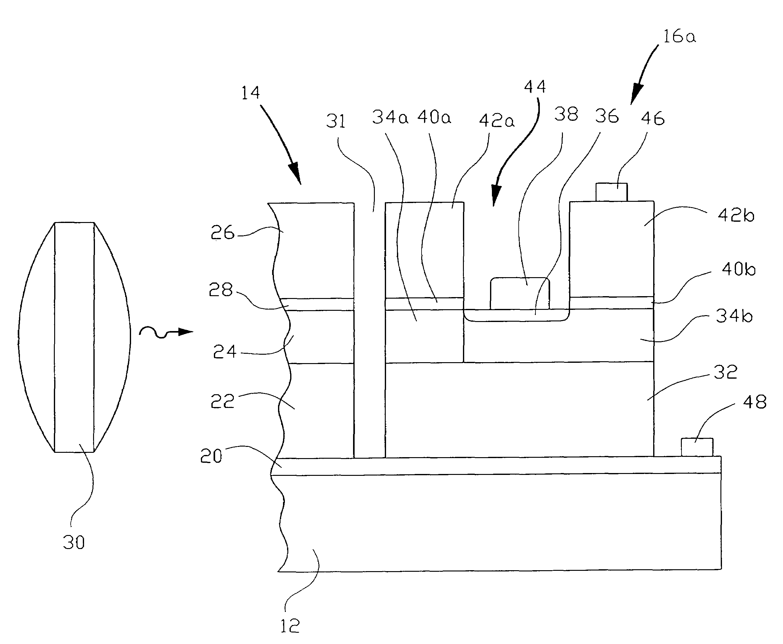
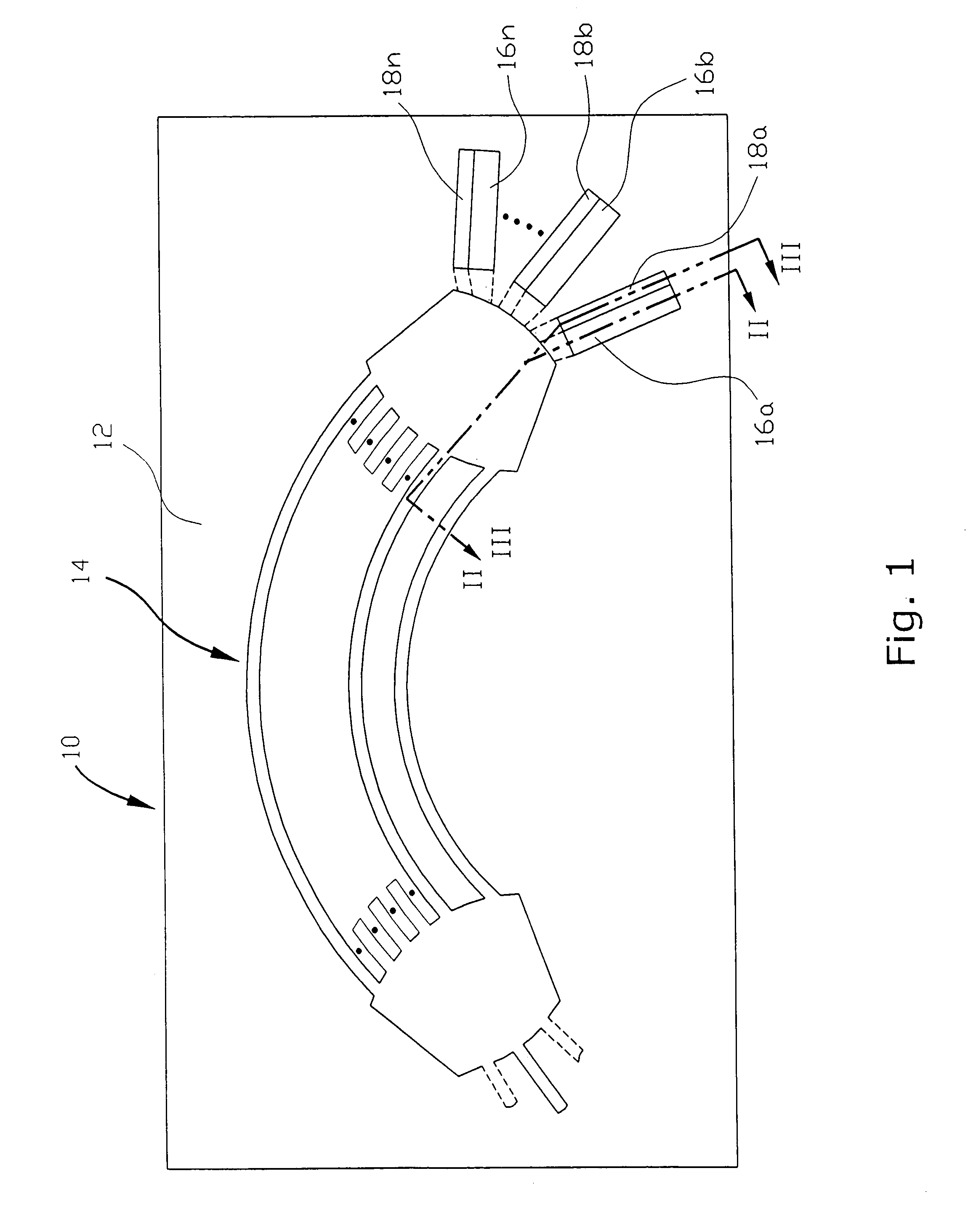
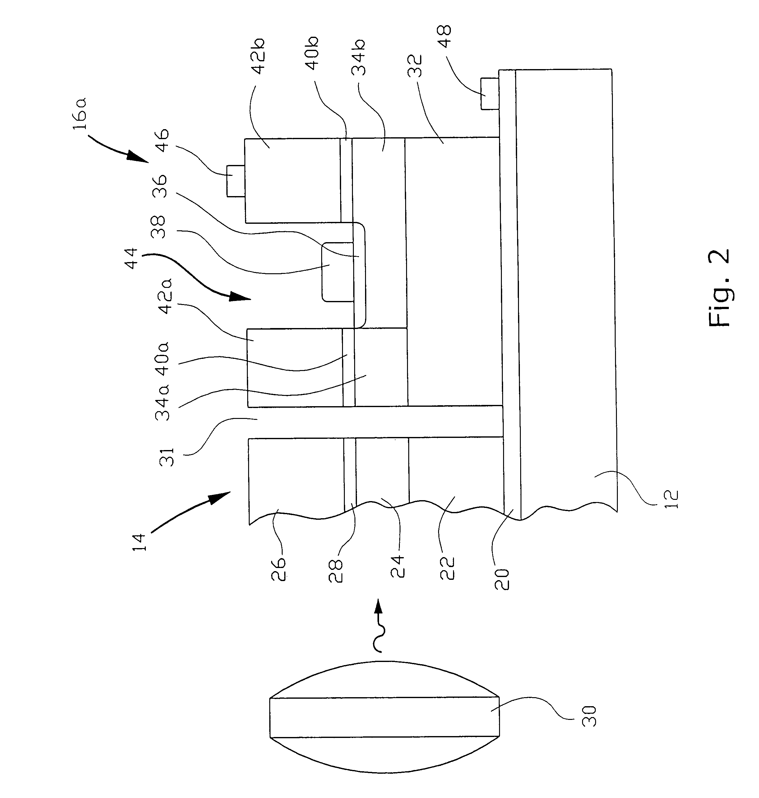
[0020]An integrated demultiplexer / photoreceiver of the present invention, which as a whole is designated by reference numeral 10, is shown in FIG. 1, which is a general top view of the device. It can be seen that the integrated demultiplexer / photoreceiver 10 (which hereinafter will be referred to as IDP) consists of the following three basic components formed on a common substrate 12: a waveguide grating routing (WGR) 14, an array of photodetectors 16a, 16b, . . . 16n, and an array of transistors 18a, 18b, . . . 18n located on the sides of the respective photodetectors 16a, 16b, . . . 16n.

[0021]As in any IDP, which incorporates a WGR as a demultiplexing component, the WGR 14 is used to demultiplex the incoming multiwavelength optical signal and to direct the individual optical channels to...


PUM


Abstract

An integrated demultiplexer / photoreceiver (IDP) for optical networks and optical interconnection devices has a common substrate which supports three sequentially arranged basic components: a waveguide grating router, an array of photodetectors, and an array of heterojunction transistors. Basic layers of all three components are grown together in a common epitaxial process, and then each of the components is individually patterned in accordance with its function. Such structure of IDP makes it possible to reduce the cost, simplify the design, improve conditions for optical alignment, and reduce optical losses. In accordance with one embodiment of the invention, transparency of the optical signal transmission layer of the WGR is controlled by selectively doping the layers of the multiple-layer waveguide structure, while in another embodiment such control is achieved by changing the width of the energy gap in the optical signal transmission layer of the WGR. Such a change is achieved by utilizing electrical bias and optical pumping from an external light source operating on a predetermined wavelength. The invention also provides a method for controlling transparency of the layer that transmits optical signals through the waveguide units in optoelectronic devices, such as an integrated demultiplexer / photoreceiver for optical network, by utilizing optical pumping and electrical bias.

Description

TECHNICAL FIELD[0001]The present invention relates to semiconductor devices, and in particular, to integrated demultiplexer / photoreceiver for optical networks and optical interconnection devices which incorporate demultiplexers in the form of wave-guide grating routing (WGR) devices, photodetectors for converting optical signals into electrical signals, and electric signals amplifiers in the form of transistors. The invention also relates to a method of controlling transparency of an optical signal transmission layer in optical signal transmission devices.BACKGROUND OF THE INVENTION[0002]At the present time, wavelength division multiplexing (WDM) optical networks (ON) and various optical interconnecting devices (OID) represent one of the fastest growing fields of technology. Among other components, a typical WDM ON incorporates a wavelength demultiplexer, which discriminates and spatially separates individual optical channels, an array of photodetectors for converting optical signal...

Claims


Application Information

Patent Timeline
Patent Type & Authority Patents(United States)
IPC IPC(8): G02B6/134H04B10/06G02B6/12G02B6/34G02B6/42
CPCG02B6/12004G02B6/42G02B6/12019
Inventor GILMAN, BORIS
Owner XONPHU LINE LIMITED LIABILITY
Why Eureka
Try Eureka