Method for fabricating semiconductor device with fine patterns

Inactive Publication Date: 2006-05-02
SK HYNIX INC
View PDF13 Cites 37 Cited by
  • Summary
  • Abstract
  • Description
  • Claims
  • Application Information

AI Technical Summary

Benefits of technology

[0020]It is, therefore, an object of the present invention to provide a method for fabricating

Problems solved by technology

Particularly, in a semiconductor device like a dynamic random access memory (DRAM) device, the design rule has been also shifted toward a trend of minimization, further resulting in a decrease in the size of semiconductor devices.
For instance, a currently fabricated semiconductor DRAM device has a minimum linewidth below about 0.1 μm, and thus, there arise many difficulties in forming semiconductor unit devices corresponding to this technical advance.
However, when the line type mask pattern, e.g., a self-aligned contact (SAC) mask pattern, is applied based on sub 0.1 μm integration technology, it is difficult to gap-fill the inter-layer insulation layer 14 between the bit lines without generating voids.
However, it is not easy to secure the

Method used


Image

  • Method for fabricating semiconductor device with fine patterns
  • Method for fabricating semiconductor device with fine patterns
  • Method for fabricating semiconductor device with fine patterns

Examples


Embodiment Construction

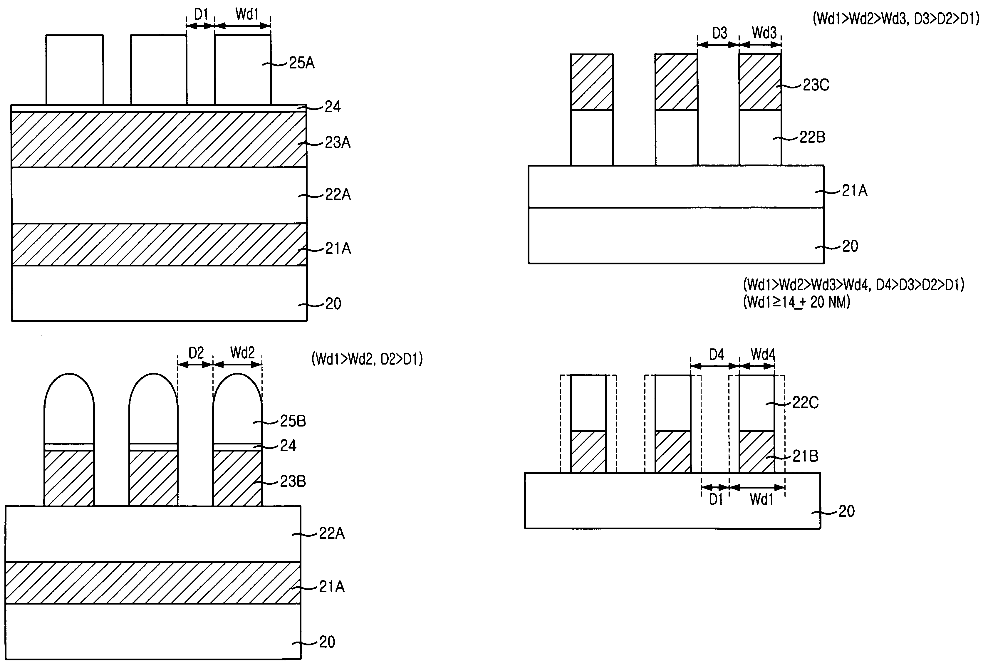
[0031]In order to minimize a linewidth of a line type conductive pattern, e.g., a bit line, etch gases and other process conditions are controlled in the course of etching an upper sacrificial hard mask containing tungsten and a nitride-based bottom hard mask. Therefore, it is possible to form fine patterns without being impacted by F2 or ArF photolithography causing severe pattern deformation.

[0032]Hereinafter, a preferred embodiment of the present invention will be described in more detail with reference to the accompanying drawings.

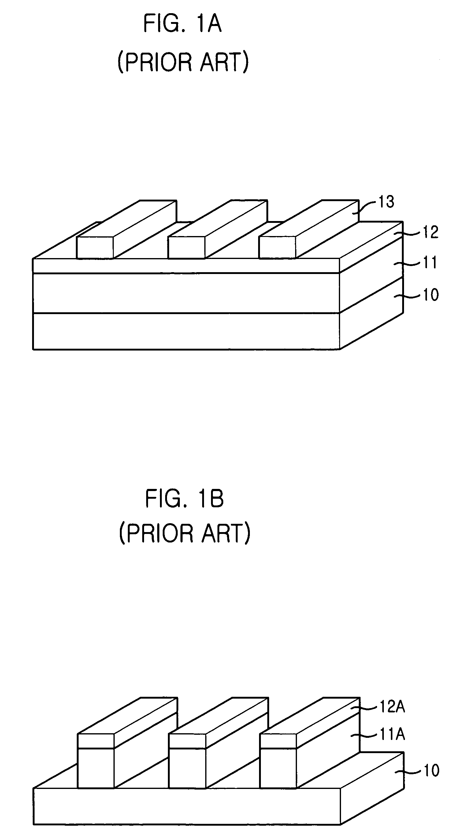
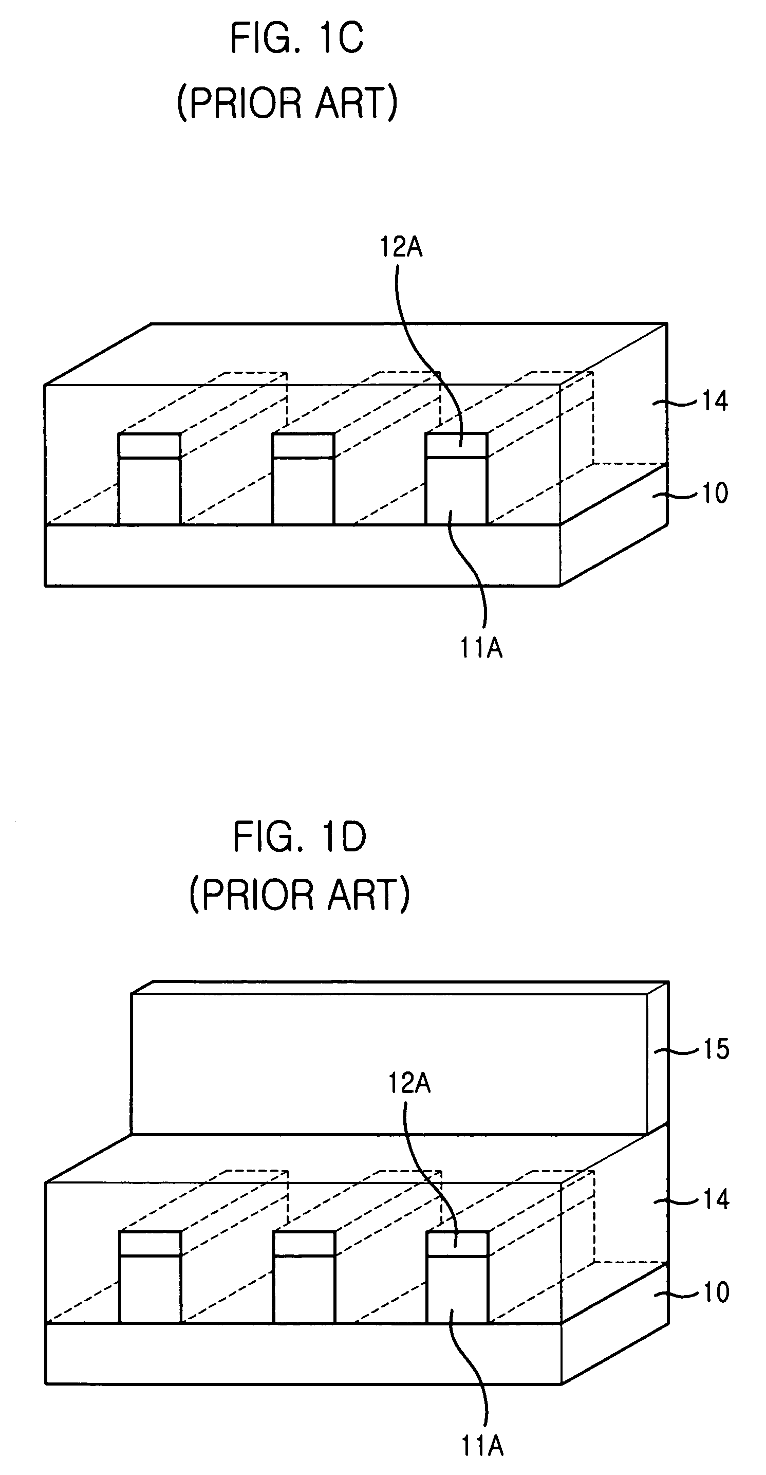
[0033]FIGS. 2A to 2D are cross-sectional views illustrating serial processes for forming line type patterns of a semiconductor device by using a light source of F2 or ArF in accordance with a preferred embodiment of the present invention.

[0034]Referring to FIG. 2A, a conductive layer 21A, which is an etch target layer, is formed on a substrate 20 providing unit devices such as a transistor and a word line. Then, an insulation layer 22A for use in a har...


PUM


Abstract

The present invention relates to a method for fabricating a semiconductor device with realizable advanced fine patterns. The method includes the steps of: forming a hard mask insulation layer on an etch target layer; forming a hard mask sacrificial layer on the hard mask insulation layer; coating a photoresist on the hard mask insulation layer; performing selectively a photo-exposure process and a developing process to form a photoresist pattern having a first width for forming a line pattern; etching selectively the hard mask sacrificial layer by using the photoresist pattern as an etch mask to form a sacrificial hard mask having a second width; removing the photoresist pattern; etching the hard mask insulation layer by controlling excessive etching conditions with use of the sacrificial hard mask as an etch mask to form a hard mask having a third width; and etching the etch target layer by using the sacrificial hard mask and the hard mask as an etch mask to form the line pattern having a fourth width, wherein the first width is wider than the fourth width.

Description

FIELD OF THE INVENTION[0001]The present invention relates to a method for fabricating a semiconductor device; and, more particularly, to a method for fabricating a semiconductor device with fine patterns.DESCRIPTION OF RELATED ARTS[0002]Large scale of integration has led semiconductor unit devices, e.g., a transistor and a capacitor, to be formed densely within a predetermined cell area. Thus, the size of the unit devices has been gradually decreased as well. Particularly, in a semiconductor device like a dynamic random access memory (DRAM) device, the design rule has been also shifted toward a trend of minimization, further resulting in a decrease in the size of semiconductor devices. For instance, a currently fabricated semiconductor DRAM device has a minimum linewidth below about 0.1 μm, and thus, there arise many difficulties in forming semiconductor unit devices corresponding to this technical advance.[0003]FIGS. 1A to 1F are perspective views illustrating a method for forming ...

Claims


Application Information

Patent Timeline
IPC IPC(8): H01L21/302H01L21/461H01L27/108H01L21/308H01L21/3213
CPCH01L21/32139H01L21/3081H10B12/00
Inventor LEE, SUNG-KWONKIM, SANG-IKLEE, MIN-SUK
Owner SK HYNIX INC
Why Eureka
Try Eureka