Semiconductor device having a multilayer interconnection structure

a multi-layer, interconnection technology, applied in the direction of semiconductor devices, semiconductor/solid-state device details, electrical apparatus, etc., can solve the problems of large dielectric constant of about 4.0, delay in signals that are transmitted through the interconnection pattern,

Inactive Publication Date: 2006-05-09
FUJITSU SEMICON LTD
View PDF29 Cites 13 Cited by
  • Summary
  • Abstract
  • Description
  • Claims
  • Application Information

AI Technical Summary

Benefits of technology

[0061]According to the present invention, the problem of short-circuit occurring in the upper layer interconnection patterns is effectively eliminated even in such a ...

Problems solved by technology

In such high-speed semiconductor integrated circuits, there occurs a problem of delay in the signals that are transmitted through the interconnection pattern of the multilayer interconnection structure as a result of the existence of stray capacitance.
On the other hand, the structure of FIG. 1C has a drawback in that the SiO2 film 12A on the organic interlayer insulation f...

Method used


Image

  • Semiconductor device having a multilayer interconnection structure
  • Semiconductor device having a multilayer interconnection structure
  • Semiconductor device having a multilayer interconnection structure

Examples


first embodiment

[0070]FIGS. 3A–3N are diagrams showing the fabrication process of a semiconductor device according to a first embodiment of the present invention.

[0071]Referring to FIG. 3A, an SiO2 film 22 is deposited on a Si substrate 21, on which an active device such as a MOSFET may be formed, by a plasma CVD process with a thickness of about 300 nm, followed by a deposition of an SiN film 23 on the SiO2 film 22 with a thickness of about 50 nm.

[0072]Next, in the step of FIG. 3B, an organic interlayer insulation film 24 of an aromatic compound polymer such as the FLARE 2.0 (trade name) of Allied Signal Corp. or a hydrocarbon polymer such as the SiLK of Dow Chemical, Inc., is deposited on the SiN film 23 by a spin-coating process, typically with a thickness of about 400 nm. Further, an organic SOG film 25 is formed on the organic interlayer insulation film 24 by a spin-coating process typically with a thickness of about 50 nm.

[0073]In the step of FIG. 3B, the interlayer insulation film 24 and the...

second embodiment

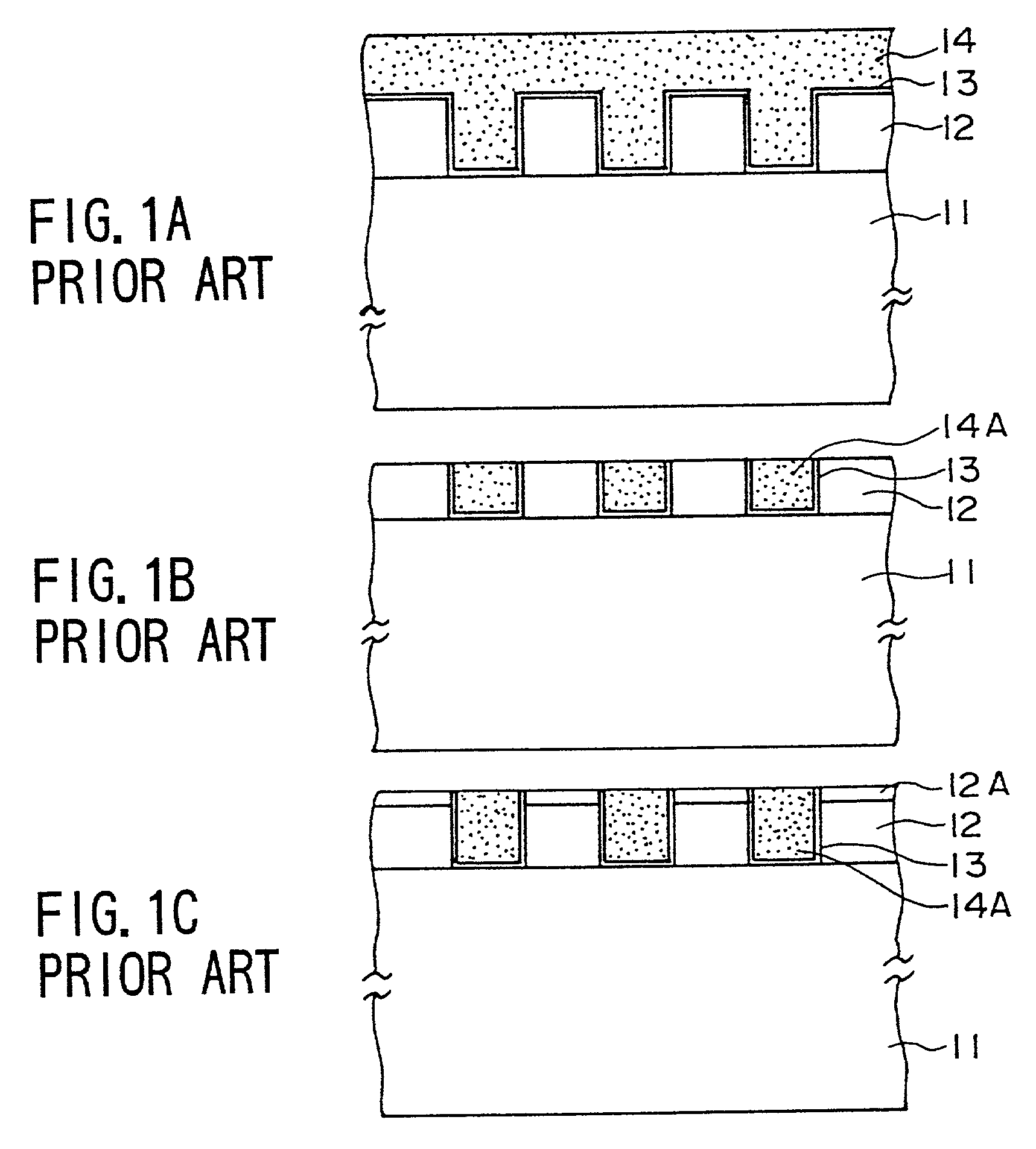
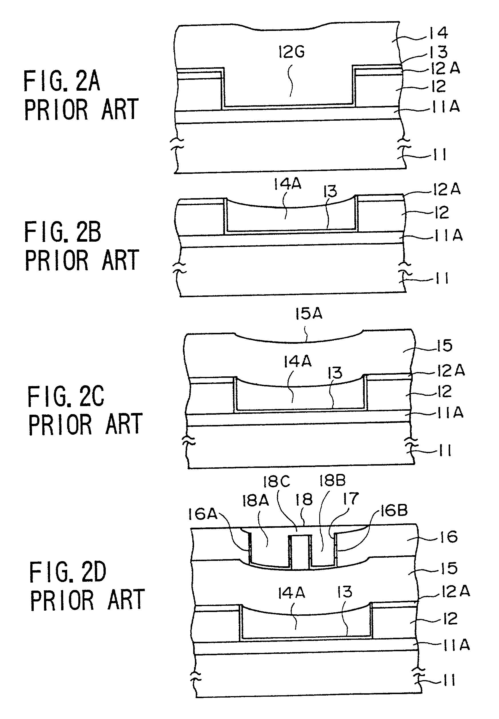
[0086]As explained with reference to FIGS. 2A–2D, there is a tendency, in a multilayer interconnection structure formed by a damascene process, that a wide conductor pattern undergoes a dishing. When such a dishing is caused, there may be a short circuit in the upper conductor patterns formed above the wide conductor pattern as explained before. Thereby, the yield of semiconductor fabrication is inevitably decreased.

[0087]Hereinafter, a fabrication process of a semiconductor device according to a second embodiment of the present invention for eliminating the foregoing problem will be described with reference to FIGS. 5A–5M.

[0088]Referring to FIG. 5A, an SiO2 film 42 is deposited on a Si substrate 41, on which an active device such as a MOSFET may be formed, by a plasma CVD process with a thickness of about 200 nm, and an organic interlayer insulation film 43 is deposited on the SiO2 film 42 by a spin-coating process typically with a thickness of about 400 nm. The organic interlayer ...

third embodiment

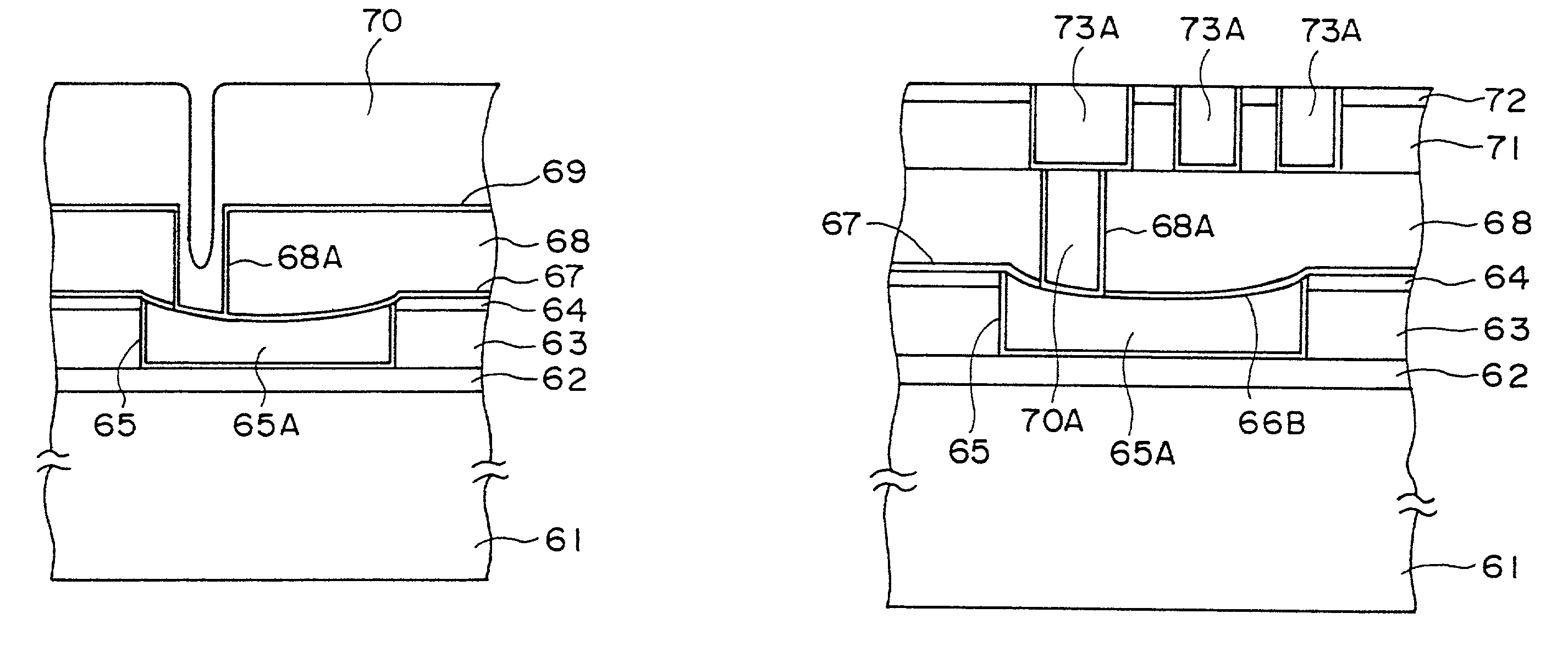
[0101]FIGS. 6A–6H show a fabrication process of a semiconductor device according to a third embodiment of the present invention.

[0102]Referring to FIG. 6A, the step of FIG. 6A corresponds to the step of FIG. 5G and an organic interlayer insulation film 63 is formed on a Si substrate 61, on which an active device such as a MOSFET is formed, via an intervening SiO2 film 62.

[0103]On the organic interlayer insulation film 63, a polishing stopper film 64 of an organic SOG film or a plasma-CVD SiO2 film is provided, and a refractory conductor film 65 of a refractory metal compound such as TiN is provided so as to cover a side wall and a bottom surface of a groove formed in the polishing stopper film 64 and the organic interlayer insulation film 63. Thereby, the groove is filled by a Cu pattern 66A formed in contact with the refractory conductor film 65 by a damascene process including a deposition of a Cu layer and a CMP process thereof, similarly as before. As a result of the chemical me...


PUM


Abstract

A semiconductor device includes a multilayer interconnection structure including an organic interlayer insulation film in which a conductor pattern is formed by a damascene process, wherein the organic interlayer insulation film carries thereon an organic spin-on-glass film.

Description

[0001]This application is a continuation of prior application Ser. No. 09 / 274,976 filed Mar. 23, 1999 now U.S. Pat. No. 6,417,116 which is hereby incorporated by reference.BACKGROUND OF THE INVENTION[0002]The present invention generally relates to semiconductor devices and more particularly to a semiconductor device having a multilayer interconnection structure and a fabrication process thereof.[0003]It is well known that the operational speed of a semiconductor device increases according to the scaling law with miniaturization of the semiconductor device. Thus, intensive efforts are being made in the art of semiconductor technology to miniaturize semiconductor devices as much as possible.[0004]Meanwhile, recent highly miniaturized, high-speed semiconductor integrated circuits generally use a multilayer interconnection structure for interconnecting individual semiconductor devices included in the integrated circuit. In such high-speed semiconductor integrated circuits, there occurs ...

Claims


Application Information

Patent Timeline
IPC IPC(8): H01L21/44H01L21/304H01L21/316H01L21/768H01L23/522H01L23/532
CPCH01L21/76802H01L21/76819H01L21/7682H01L21/76829H01L21/76834H01L21/76835H01L21/76837H01L21/7684H01L21/76882H01L23/5222H01L23/5329H01L2924/0002H01L23/53228H01L2924/12044H01L2924/00H01L23/53295H01L23/53238H01L21/31
Inventor KUDO, HIROSHIIKEDA, MASANOBUWATANABE, KENICHIOHKURA, YOSHIYUKI
Owner FUJITSU SEMICON LTD
Why Eureka
Try Eureka