Method of making heterojunction P-I-N diode

a technology of p-i-n diodes and heterojunction, applied in the field of heterojunction semiconductor devices, can solve the problems of reducing the performance characteristics of present p-i-n switching diodes, reducing the insertion loss without compromising, and not considering the gain, etc., to achieve the effect of reducing the series resistan

Inactive Publication Date: 2006-05-23
MACOM TECH SOLUTIONS HLDG INC
View PDF23 Cites 9 Cited by
  • Summary
  • Abstract
  • Description
  • Claims
  • Application Information

AI Technical Summary

Benefits of technology

[0006]According to an aspect of the invention, a heterojunction P-I-N diode comprises a first layer of doped semiconductor material of a first doping type; a second layer of doped semiconductor material of a second doping type and a substrate on which is disposed the first and second layers. An intrinsic layer of semiconductor material is disposed between the first layer and second layer. The semiconductor material composition of at least one of the first layer and second layer is sufficiently different from that of the intrinsic layer so as to form a heterojunction therebetween. An energy barrier is created in which injected carriers from the junction are confined by the barrier, effectively reducing the series resistance within the I region of the P-I-N diode and the insertion loss relative to that of homojunction P-I-N diodes.

Problems solved by technology

Performance characteristics of present P-I-N switching diodes are often limited by parameters such as insertion loss and isolation.
A significant problem for P-I-N diode designers is how to reduce insertion loss without compromising isolation.
For diode switch design, however, gain is not a consideration.

Method used


Image

  • Method of making heterojunction P-I-N diode
  • Method of making heterojunction P-I-N diode
  • Method of making heterojunction P-I-N diode

Examples


Embodiment Construction

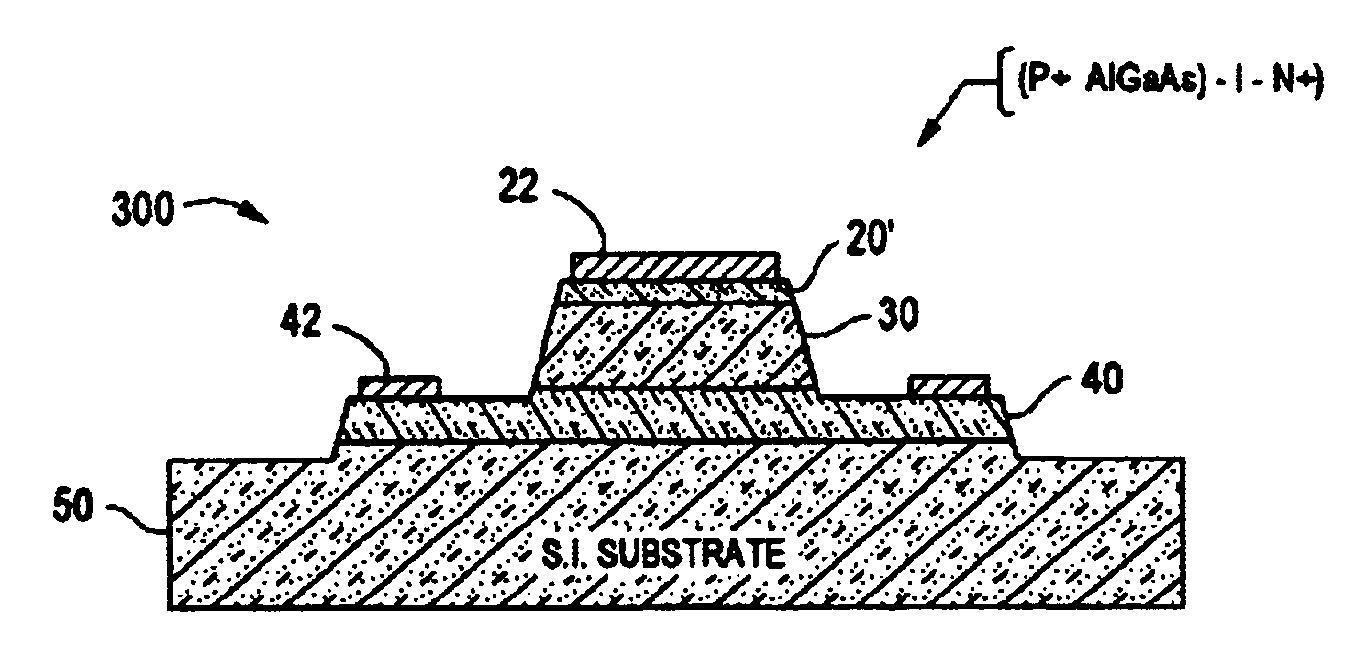
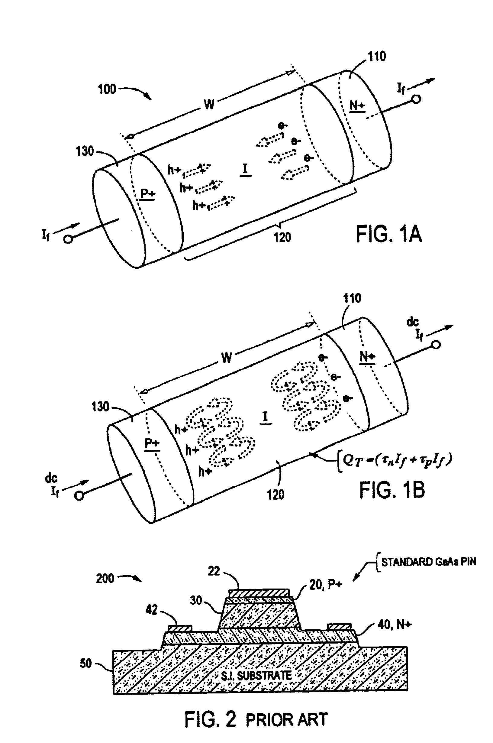
[0024]Referring now to FIGS. 1A and 1B, the basic theory of operation of P-I-N diodes will be briefly described. Throughout the drawings, like reference numerals are used to indicate like parts. P-I-N diode 100 comprises an intrinsic layer 120 of semiconductor material coupled between a layer 130 of P+ doped semiconductor material and a layer 110 of N+ semiconductor material. FIG. 1A illustrates schematically the diffusion of electrons (e) and holes (h) across the intrinsic (I) layer of width w upon application of a current source If to the two terminal device at low frequency operation (DC to ft). In this mode of operation, the current flow through the device may be described by the well-known diode equation I=I0(eq(Va−IRs) / nkT)−1). Operation of the P-I-N diode in this region may be characterized by a rectified RF voltage signal and a high loss non-linear device.

[0025]FIG. 1B illustrates schematically the high frequency operation (f0>ft) of a diode device where the transition frequ...


PUM


Abstract

A heterojunction P-I-N diode switch comprises a first layer of doped semiconductor material of a first doping type, a second layer of doped semiconductor material of a second doping type and a substrate on which is disposed the first and second layers. An intrinsic layer of semiconductor material is disposed between the first layer and second layer. The semiconductor material composition of at least one of the first layer and second layer is sufficiently different from that of the intrinsic layer so as to form a heterojunction therebetween, creating an energy barrier in which injected carriers from the junction are confined by the barrier, effectively reducing the series resistance within the I region of the P-I-N diode and the insertion loss relative to that of homojunction P-I-N diodes.

Description

CROSS REFERENCE TO RELATED APPLICATIONS[0001]This application is a divisional application of U.S. patent application Ser. No. 10 / 139,067, filed May 3, 2002, now U.S. Pat. No. 6,794,734.FIELD OF THE INVENTION[0002]This invention relates generally to semiconductor devices, and more particularly to heterojunction semiconductor devices.BACKGROUND OF THE INVENTION[0003]P-I-N diodes are often used as switching elements in a variety of military and commercial applications. Such applications include automotive collision avoidance systems (CAS), passive radiation imaging systems and radar applications, and switch matrix devices useful for networking (e.g. internet) applications. Presently, P-I-N diodes used in such RF and microwave applications are fabricated as homojunction devices, such as silicon (Si) or gallium arsenide (GaAs) P-I-N diodes. These devices may be used as either discrete or as integrated components for switching functions useful at high frequency operation. Such high freque...

Claims


Application Information

Patent Timeline
Patent Type & Authority Patents(United States)
IPC IPC(8): H01L21/332H01L29/861H01L29/868
CPCH01L29/868H01L29/0657H01L29/20Y02E10/548
Inventor HOAG, DAVID RUSSELLBOLES, TIMOTHY EDWARDBROGLE, JAMES JOSEPH
Owner MACOM TECH SOLUTIONS HLDG INC
Why Eureka
Try Eureka