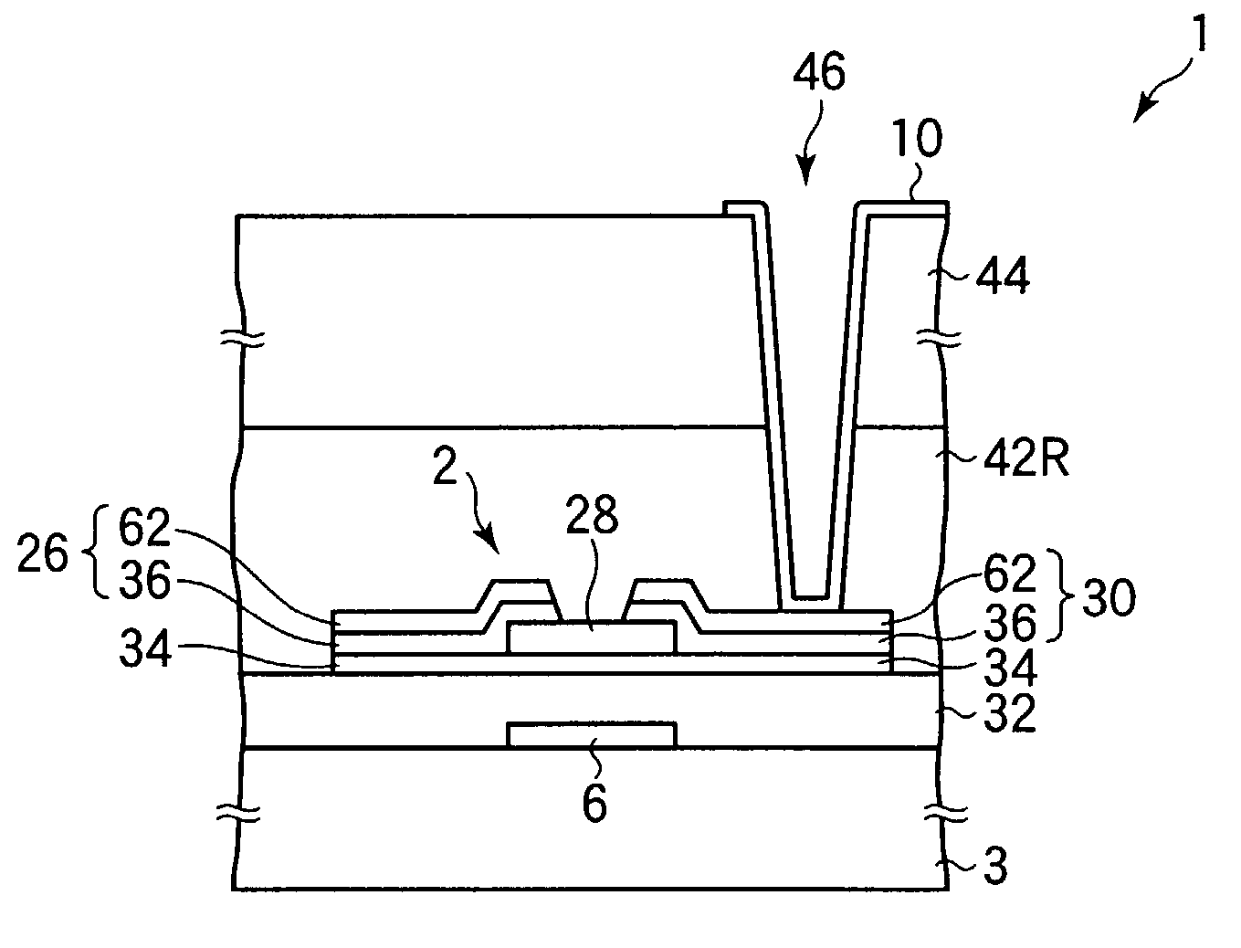
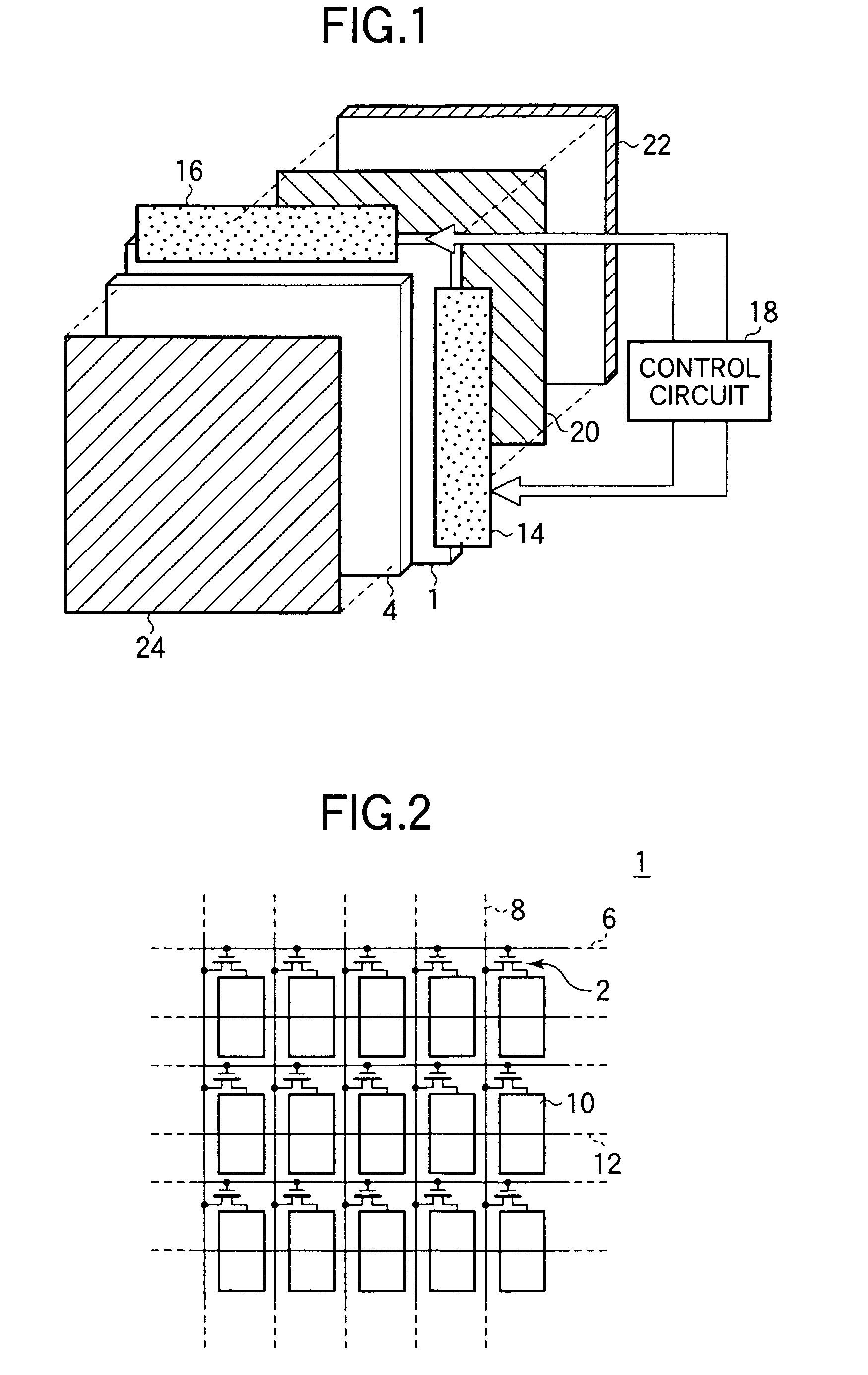
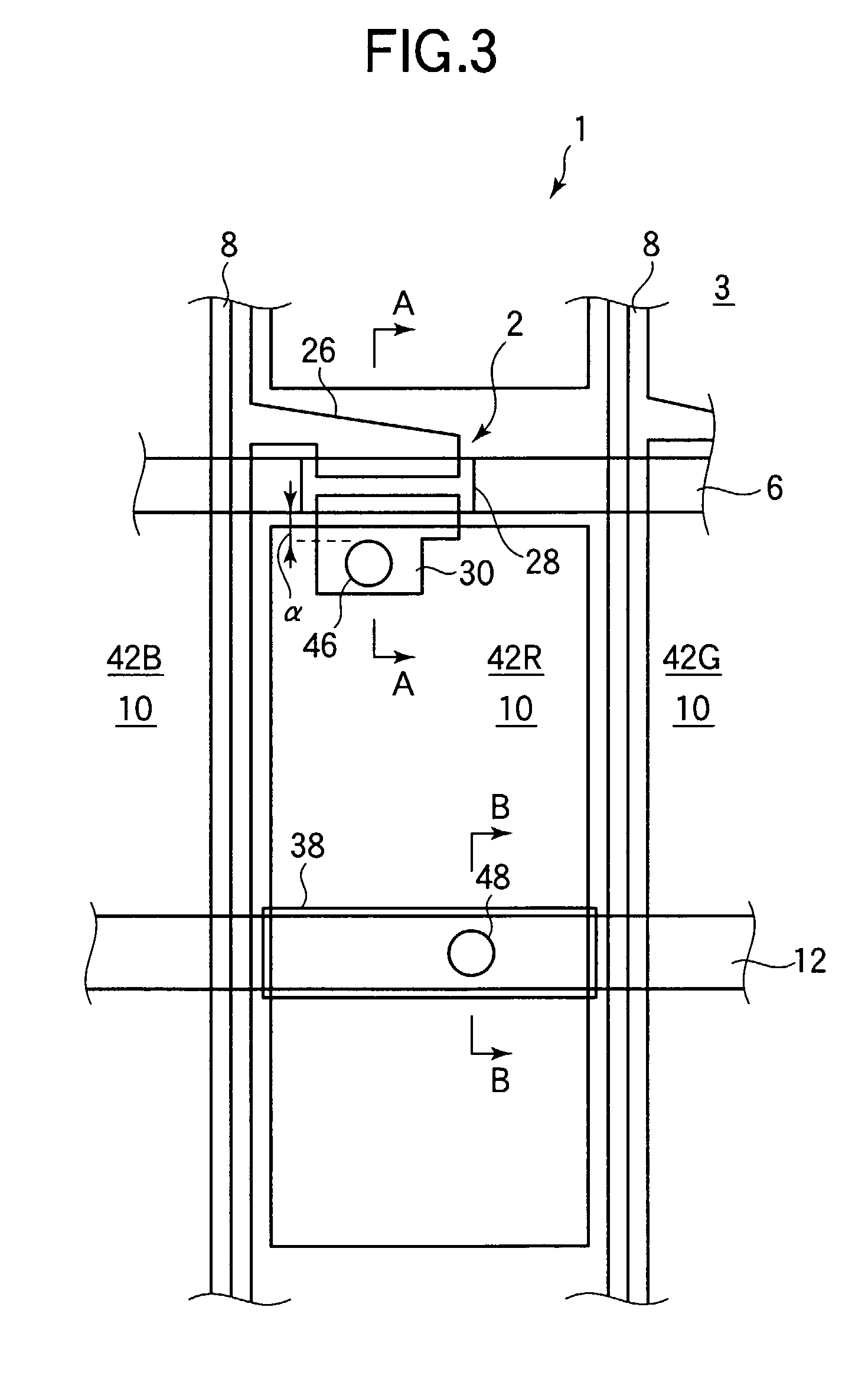
[0026]The present invention has an object to provide a substrate for use in a liquid
crystal display, which can simplify a manufacturing process typified by a
photolithography process and has high reliability, a method for manufacturing the same, and a liquid
crystal display using the same.
[0028]When a resin layer is formed on the whole surface of the substrate, and an electrode wiring line made of, for example, a transparent
oxide electrode material or the like is formed on the resin layer, the adhesion of the wiring line or the like to the resin layer is often inferior to that to a glass substrate, and there is a case where peeling occurs. The peeling of the wiring line or the like can be suppressed by opening the resin layer and patterning while the wiring line or the like is brought into direct contact with the glass substrate. In the case where the opening portion of the resin layer has a linear shape, there is a case where a stepped portion is steep and an
etching residual substance of a transparent
oxide electrode material or the like is generated between the electrode wiring lines. On the other hand, when an opening pattern of the resin layer between electrode terminals is made a shape with a sharpened tip, the shape of the stepped portion of the selection portion is moderated and the generation of the
etching residual substance can be suppressed.
[0029]In the CF-on-TFT structure in which the opposite electrode does not have a light shielding film, an intense light leakage from a backlight unit is problematic in the frame region of the periphery of a display region. Thus, in the frame portion, it is necessary to block out the light by superposition of resins of two or more colors. However, in the construction provided with the overcoat (OC) layer, the frame region has the film thickness of a laminate of the two-layer lamination CF layer and the OC layer, and becomes higher than the film thickness of the CF layer of one layer and the OC layer in the display region whereby a difference in level becomes large. The
cell thickness of the liquid crystal is changed by this, and display unevenness, the so-called frame unevenness, is produced. In order to deal with this, an opening region is provided such that three
layers of CF resin are laminated in the frame region, and the OC layer is not formed in the region. Then, the frame region is exposed to
etching of the gate insulating film or the like, so that the uppermost CF layer of the CF resin stacked portion is removed by the etching and the film thickness of the whole frame region is made two
layers of the resin CF
layers +α, and whereby formation of a noticeable stepped portion relatively to the display region can be prevented.
[0036]To these problems, for example, by providing an opening pattern on a storage
capacitance electrode, and further providing a similar opening pattern on the CF layer of the upper layer, it is possible to eliminate the absorption of the incident light by the CF layer, which becomes an obstacle to automatic focusing, and the superposition of the opening pattern of the storage
capacitance electrode and the opening pattern opened in the pixel electrode can be measured.
[0037]With respect to the shape of the
contact hole for electrically connecting the source electrode of the TFT and the pixel electrode, when the relation between diameters of contact holes of the CF layer, the SiN layer and the OC layer existing over the source electrode is made CF layer>SiN layer>OC layer, a structure can be formed such that the CF resin is covered with the OC layer in the vertical direction, and it is possible to remove the influence of
pollution due to the
pigment or the like in the resin CF layer upon the liquid crystal or the TFT.
[0042]The positional relation between the resin film and the
contact hole is important, and the occurrence of the crack can be suppressed when the distance of the pixel edge portion is made 2.5 or more times as large as the film thickness of the OC layer, the distance of a taper portion at the end of the
contact hole is made 1.5 or more times as large as the film thickness, or the angle is made 45° or less.


