Semiconductor device and manufacturing method thereof

a technology of semiconductor devices and manufacturing methods, applied in semiconductor devices, semiconductor/solid-state device details, electrical apparatus, etc., can solve the problems of cracking in the bonding pad or the insulating film, etc., to reduce the manufacturing cost of the second pad, the effect of resisting the second pad and enhancing the electrical connection between the first pad and the third pad

Active Publication Date: 2019-03-19
SEIKO EPSON CORP
View PDF12 Cites 0 Cited by
  • Summary
  • Abstract
  • Description
  • Claims
  • Application Information

AI Technical Summary

Benefits of technology

[0008]According to the first aspect of the invention, a pad having a multilayer structure can be configured by a plurality of metal plates including the first to third pads, and as a result, the mechanical strength of a pad can be improved more than before, and the occurrence of a crack can be suppressed. Also, the second pad is formed so as to have a film thickness that is smaller than the film thickness of the insulating layer, and therefore, the second pad need not be thinned through polishing. Furthermore, as a result of forming the first and second pads at the same time a metal interconnect or a plug is formed, such a semiconductor device can be manufactured without adding new processes to a common manufacturing method of a semiconductor device.
[0019]Also, the first pad may be arranged on an interlayer insulating film that includes FSG (fluorine-doped silicate glass) or a low-k material. By using such an interlayer insulating film, although the parasitic capacitance of the pad can be reduced, the mechanical strength of the interlayer insulating film decreases. However, in the case of using the pad having a multilayer structure, even if the mechanical strength of the interlayer insulating film is low, the mechanical strength of the pad can be improved, and the occurrence of a crack can be suppressed.

Problems solved by technology

However, the copper wire has higher hardness compared with a gold wire and an aluminum pad, and there are cases where a pad does not have a strength that is sufficient to endure mechanical stress that is applied when the wire is bonded thereto, and therefore, a crack occurs in the pad or an interlayer insulating film.
Accordingly, particularly in the case of using a copper bonding wire, a crack may occur in the bonding pad or the insulating film when the bonding wire is joined to the bonding pad.

Method used


Image

  • Semiconductor device and manufacturing method thereof
  • Semiconductor device and manufacturing method thereof
  • Semiconductor device and manufacturing method thereof

Examples


Embodiment Construction

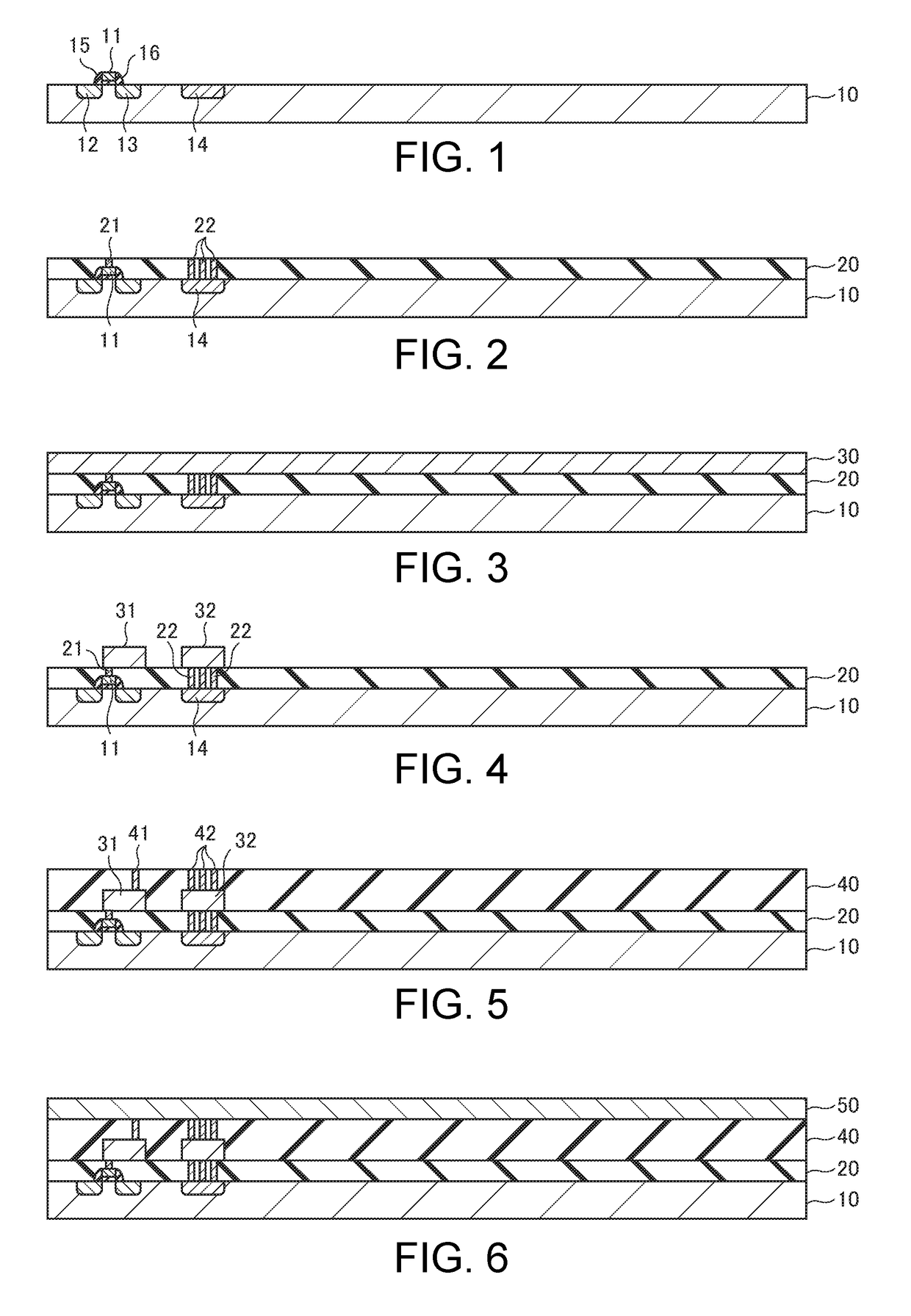
[0038]Hereinafter, an embodiment of the invention will be described in detail with reference to the drawings. The same constituent elements are given the same reference numerals, and redundant descriptions are omitted.

[0039]Manufacturing Method of Semiconductor Device

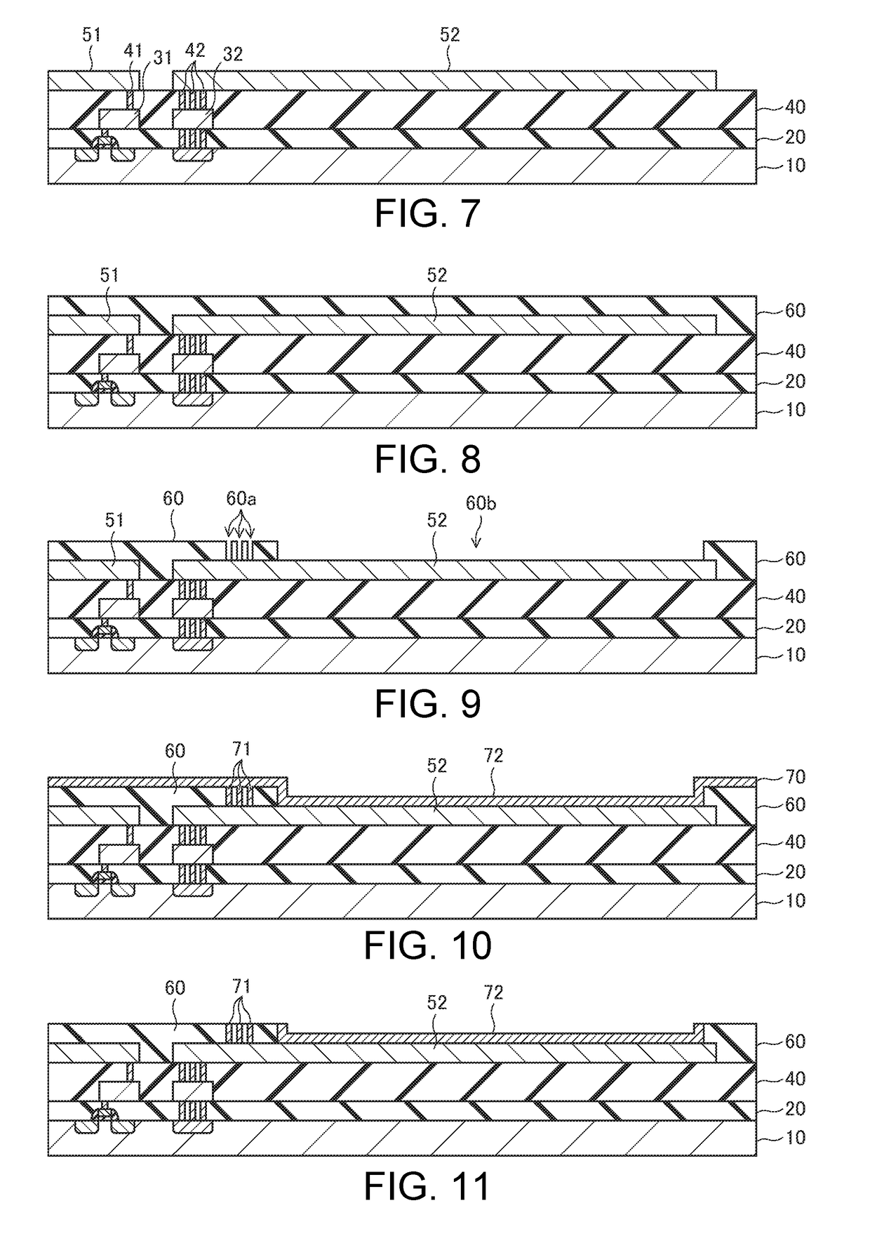
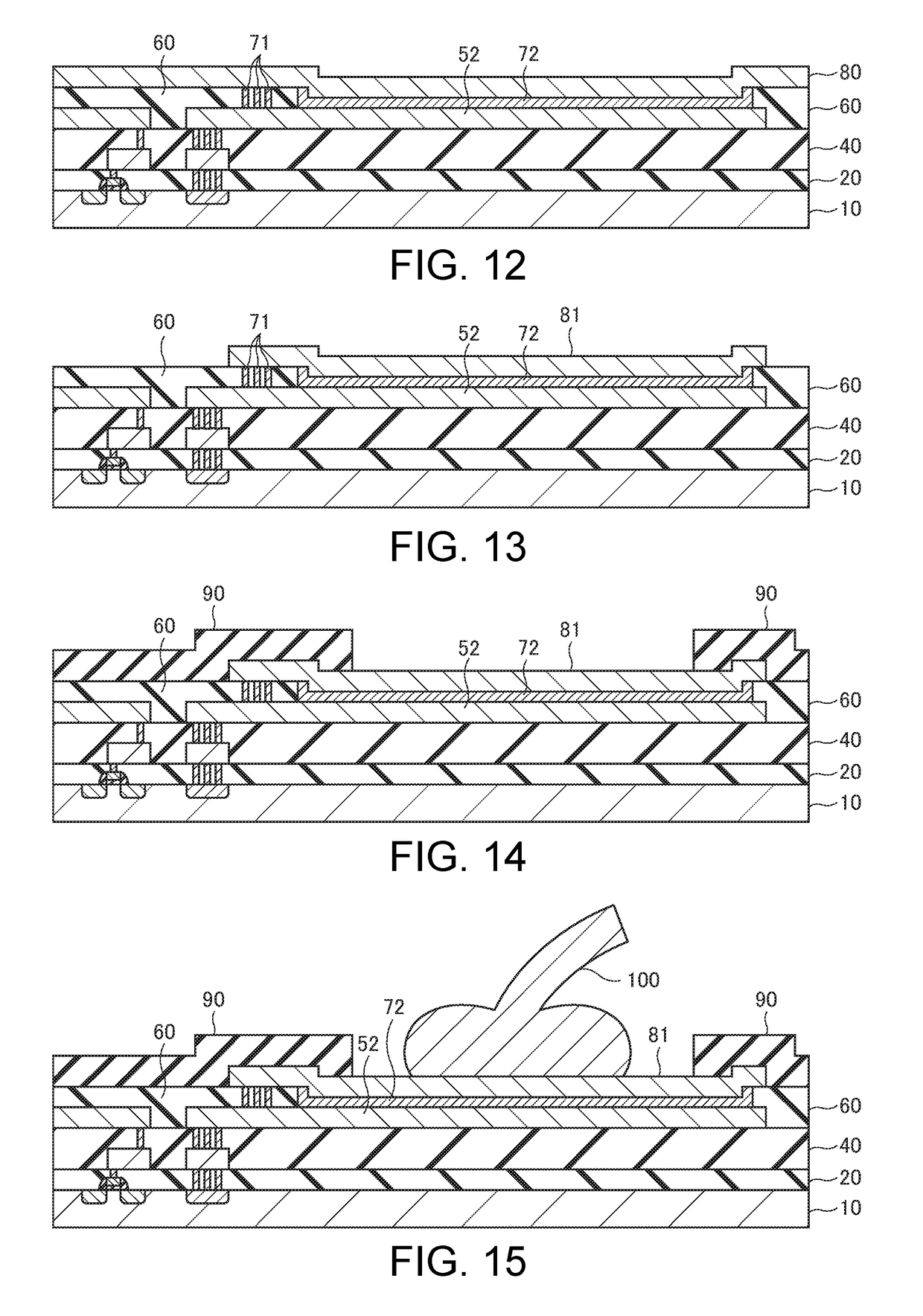
[0040]FIGS. 1 to 15 are cross-sectional views, in a manufacturing process, of a semiconductor device according to one embodiment of the invention. In the following, a case where a semiconductor device including an N-channel MOS transistor is manufactured using a P-type semiconductor substrate will be described as an example.

[0041]In a first step, as shown in FIG. 1, a gate electrode 11 is formed on a semiconductor substrate 10 via a gate insulating film, the gate electrode 11 being patterned using a photolithography method. For example, the semiconductor substrate 10 is made of silicon (Si) including P-type impurities such as boron (B) ions or the like. The gate insulating film is made of silicon oxide (SiO2) or the lik...


PUM

PropertyMeasurementUnit
thicknessaaaaaaaaaa
Young's modulusaaaaaaaaaa

Abstract

The manufacturing method of a semiconductor device can improve the mechanical strength of a pad more than before, and suppress the occurrence of a crack. The manufacturing method of a semiconductor device includes: forming a first pad constituted by a first metal layer; forming an insulating layer on the first pad; providing an opening portion in the insulating layer by removing the insulating layer on at least a partial region of the first pad; forming a second pad constituted by a second metal layer in the opening portion of the insulating layer so as to have a film thickness that is smaller than the film thickness of the insulating layer; and forming a third pad constituted by a third metal layer on the second pad.

Description

BACKGROUND1. Technical Field[0001]The present invention relates to semiconductor devices, manufacturing methods thereof, and the like.2. Related Art[0002]Aluminum (Al) or an aluminum alloy, in general, is used as a material for metal interconnects that are formed in a semiconductor chip that constitutes a semiconductor device. In the semiconductor chip, partial regions of the metal interconnects constitute pads (terminals) that are electrically connected to an external member for power supply and signal transmission. For example, in the case of a semiconductor chip that has a multilevel interconnection structure, partial regions of the metal interconnects in the uppermost level that are formed on an interlayer insulating film constitute pads.[0003]Furthermore, pads of the semiconductor chip are electrically connected to terminals or electrodes of a semiconductor package, a printed circuit board, or the like, by wire bonding. Heretofore, a gold (Au) wire has been used in wire bonding...

Claims


Application Information

Patent Timeline
Patent Type & Authority Patents(United States)
IPC IPC(8): H01L23/522H01L23/00H01L23/532H01L23/485H01L21/768
CPCH01L23/5226H01L21/76802H01L21/76877H01L23/485H01L24/03H01L24/05H01L24/85H01L24/06H01L2224/48463H01L23/5329H01L23/53214H01L23/53257H01L2224/05553H01L2224/0612H01L21/4853H01L23/49811H01L24/45H01L2224/02166H01L2224/05624H01L2224/45144H01L2224/45147H01L2224/85045H01L2224/85203H01L2224/85205H01L2224/48227H01L2224/85207H01L2924/3512H01L2224/05124H01L2224/05184H01L2224/05082H01L2224/05095H01L2224/05096H01L24/48H01L2224/48824H01L2224/034H01L2224/03602H01L2924/00014H01L2924/01029H01L2924/01014
Inventor YOSHIZAWA, TAKAHIKOWATANABE, KUNIOSHIRASAWA, TATSUKISAKUDA, TAKASHI
Owner SEIKO EPSON CORP
Why Eureka
Try Eureka