Semiconductor laser device and method for manufacturing the same

a semiconductor and laser technology, applied in laser optical resonator construction, laser cooling arrangements, laser details, etc., can solve the problems of reducing yield, difficult to achieve single longitudinal mode characteristics with high yield, and complex manufacturing processes

Inactive Publication Date: 2006-05-23
PANASONIC CORP
View PDF12 Cites 0 Cited by
  • Summary
  • Abstract
  • Description
  • Claims
  • Application Information

AI Technical Summary

Benefits of technology

[0026]A method for manufacturing this second DBR semiconductor laser device of the present invention includes forming the current blocking layer on the active layer, partially removing the current blocking layer to form the stripe-shaped window, and forming the diffraction

Problems solved by technology

However, these conventional structures pose the following problems:(1) The etching for the formation of the stripe-shaped window 109a degrades the shape of the diffraction grating 106a, and it is difficult to achieve single longitudinal mode characteristics with high yield.(2) In the portion in which the thickness of the diffraction grating layer 109 has become thinner due to the formation of the diffraction grating 106a, over-etching may occur when forming the stripe-shaped window, and the etching may reach the first optical guiding layer 105 below the diffraction grating layer 106, reducing the yield.(3) When the diffraction grating layer 106 is formed below the active layer 104, the diffraction grating is no longer exposed to the etching, but in that case the active layer 104 is formed on

Method used


Image

  • Semiconductor laser device and method for manufacturing the same
  • Semiconductor laser device and method for manufacturing the same
  • Semiconductor laser device and method for manufacturing the same

Examples


first embodiment

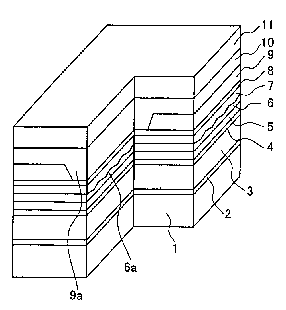
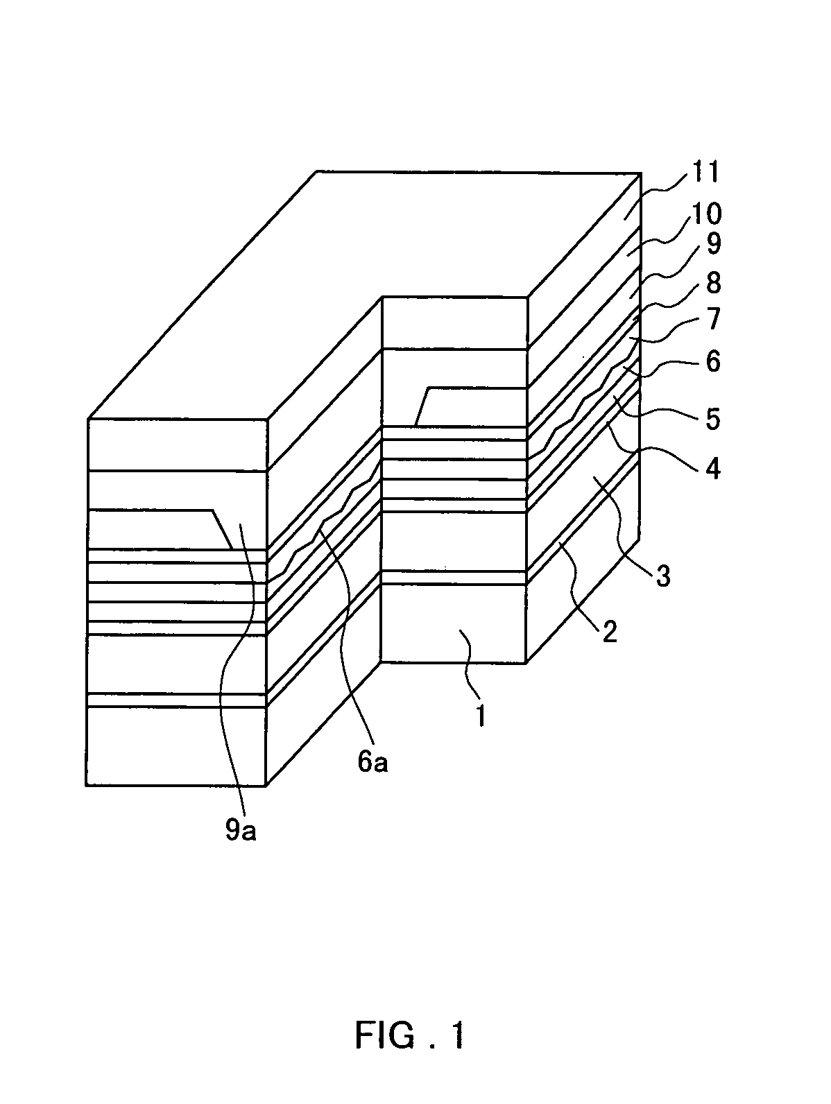
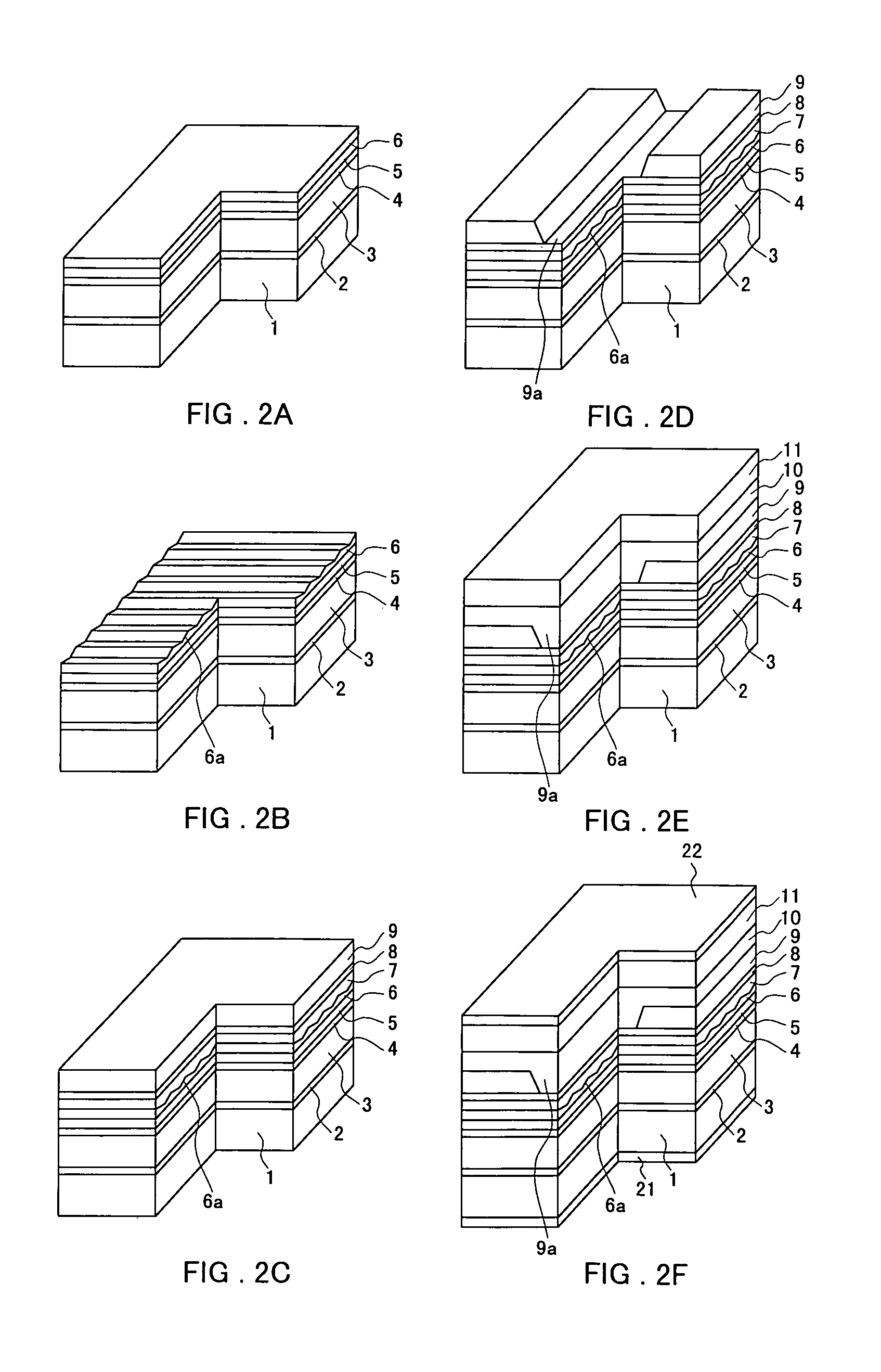
[0040]In the DFB semiconductor laser shown in FIG. 1, an n-type GaAs buffer layer 2, an n-type Ga0.5Al0.5As first cladding layer 3, a Ga0.85Al0.15As active layer 4, a p-type Ga0.5Al0.5As first optical guiding layer 5, a p-type Ga0.8Al0.2As diffraction grating layer 6, a p-type Ga0.5Al0.5As second optical guiding layer 7, and a p-type Ga0.8Al0.2As etch-stop layer 8 are formed in that order on top of an n-type GaAs substrate 1. Formed on top of that layering structure is an n-type Ga0.4Al0.6As current blocking layer 9 having a stripe-shaped window 9a for current confinement. Furthermore, a p-type Ga0.5Al0.5As second cladding layer 10 and a p-type GaAs contact layer 11 are formed on the current blocking layer 9 and the stripe-shaped window 9a.

[0041]In this laser device, the current injected from the p-type GaAs contact layer 11 is confined by the n-type Ga0.4Al0.6As current blocking layer 9 in the stripe-shaped window 9a, and laser oscillation in the 780 nm band occurs in the active l...

second embodiment

[0059]FIG. 3 shows a DBR semiconductor laser device in accordance with a second embodiment of the present invention. As shown in FIG. 3, in this semiconductor laser, the diffraction grating 6a is formed only at a distributed reflection region B of the diffraction grating layer 6. The method for manufacturing this structure is the same as for the first embodiment up to the formation of the p-type Ga0.8Al0.2As diffraction grating layer 6 in the first crystal growth process. Then, as shown in FIG. 4, the diffraction grating 6a is formed only in the distributed reflection region B by etching only the distributed reflection region B and not the active region A in the surface of the diffraction grating layer 6. In this embodiment, the length of the active region was set to 500 μm, and the length of the distributed reflection region was set to 300 μm.

[0060]Next, as in the first embodiment, a second optical guiding layer 7, an etch-stop layer 8, and a current blocking layer 9 are formed. Af...

third embodiment

[0062]FIG. 5 shows a DBR semiconductor laser device in accordance with a third embodiment of the present invention. In this semiconductor structure, the second cladding layer 10 is provided with a ridge shape, and for current confinement, an n-type Ga0.4Al0.6As current blocking layer 9 is formed in the region outside the ridge serving as a current channel. Numeral 12 denotes a p-type GaAs protective layer, and numeral 11 denotes a p-type GaAs contact layer.

[0063]A method for manufacturing this semiconductor laser is shown in FIG. 6. First, as in the first and second embodiments, the layers up to the diffraction grating layer are formed in a first crystal growth process, then the diffraction grating 6A is formed, and the layers up to the protective layer 12 are formed in a second crystal growth process, as shown in FIG. 6A.

[0064]Then, as shown in FIG. 6B, a stripe-shaped dielectric film 13, for example of nitride (silicon nitride or tungsten nitride) or silicon oxide, is formed, and ...


PUM


Abstract

The invention provides a semiconductor laser device including an active layer, a semiconductor layer provided with a diffraction grating, an etch-stop layer, a cladding layer provided with a stripe structure, and a current blocking layer arranged at least on a side of said stripe structure, formed in that order on a substrate. In this semiconductor laser device, the etching-stop layer is formed on the semiconductor layer with the diffraction grating, so that damage of the diffraction grating due to etching can be prevented. The invention also provides a distributed Bragg reflection semiconductor laser device, including an active layer, and a current blocking layer having a stripe-shaped window and a diffraction grating formed at least near an end face thereof. This semiconductor laser device can be manufactured with fewer crystal growth processes than conventional semiconductor laser devices.

Description

BACKGROUND OF THE INVENTION[0001]1. Field of the Invention[0002]The present invention relates to distributed feedback semiconductor lasers and distributed Bragg reflector semiconductor lasers.[0003]2. Description of the Related Art[0004]Distributed feedback (referred to as “DFB” in the following) and distributed Bragg reflector (referred to as “DBR” in the following) are two well-known structures for semiconductor lasers, in which oscillation in a single longitudinal mode is achieved by employing a diffraction grating with excellent wavelength selectivity in the semiconductor optical waveguide. To use such semiconductor lasers as light sources for optical information processing or optical measurements, a so-called transversal mode control is necessary to ensure that the laser oscillates in the basic transversal mode.[0005]For DFB semiconductor lasers, a structure for transversal mode control and current confinement is known, in which a stripe-shaped recess portion (so-called window)...

Claims


Application Information

Patent Timeline
IPC IPC(8): H01S5/00H01S5/20H01S5/223H01S5/12H01S5/323
CPCH01S5/12H01S5/2231H01S5/32316H01S5/209
Inventor ORITA, KENJIMOCHIDA, ATSUNORIYURI, MASAAKI
Owner PANASONIC CORP
Why Eureka
Try Eureka