Method of fabricating an interconnect structure employing air gaps between metal lines and between metal layers

a technology of air gaps and interconnect structures, applied in the field of new interconnect structures and methods for forming integrated circuits, can solve the problems of undesirable rc delay, rc delay, signal propagation delay, etc., and achieve the effect of reducing parasitic capacitan

Inactive Publication Date: 2006-06-06
NEWPORT FAB
View PDF14 Cites 39 Cited by
  • Summary
  • Abstract
  • Description
  • Claims
  • Application Information

AI Technical Summary

Benefits of technology

[0010]It is an object of the present invention to provide an improved interconnect structure that red

Problems solved by technology

RC delay is the propagation delay of a signal caused by resistance in metal lines and the capacitance between metal lines and between metal layers.
RC delay is undesirable because this delay adversely affects timing requirements and the performance of the circuit design by injecting uncertainty as to when a signal will be received or valid at a particular node in the circuit.
Cross-talk is the signal interference between metal lines that can adversely affect signal integrity and signal strength.
It is apparent that RC delay problems, cross-talk issues, and power dissipation stem mainly from interconnect intra-layer capacitance (i.e., capacitance between metal lines within a metal layer) and interconnect inter-layer capacitance (i.e., capacitance between metal layers).
First, the deposition of porous materials is complicated and difficult to control.
Second, the porous materials generally provide poor mechanical strength.
Third, the porous materials generally provide poor thermal conductivity.
Fourth, because of the porous nature of these materials, defining via holes or trenches with smooth vertical walls and bottom surfaces therein is a di

Method used


Image

  • Method of fabricating an interconnect structure employing air gaps between metal lines and between metal layers
  • Method of fabricating an interconnect structure employing air gaps between metal lines and between metal layers
  • Method of fabricating an interconnect structure employing air gaps between metal lines and between metal layers

Examples


first embodiment

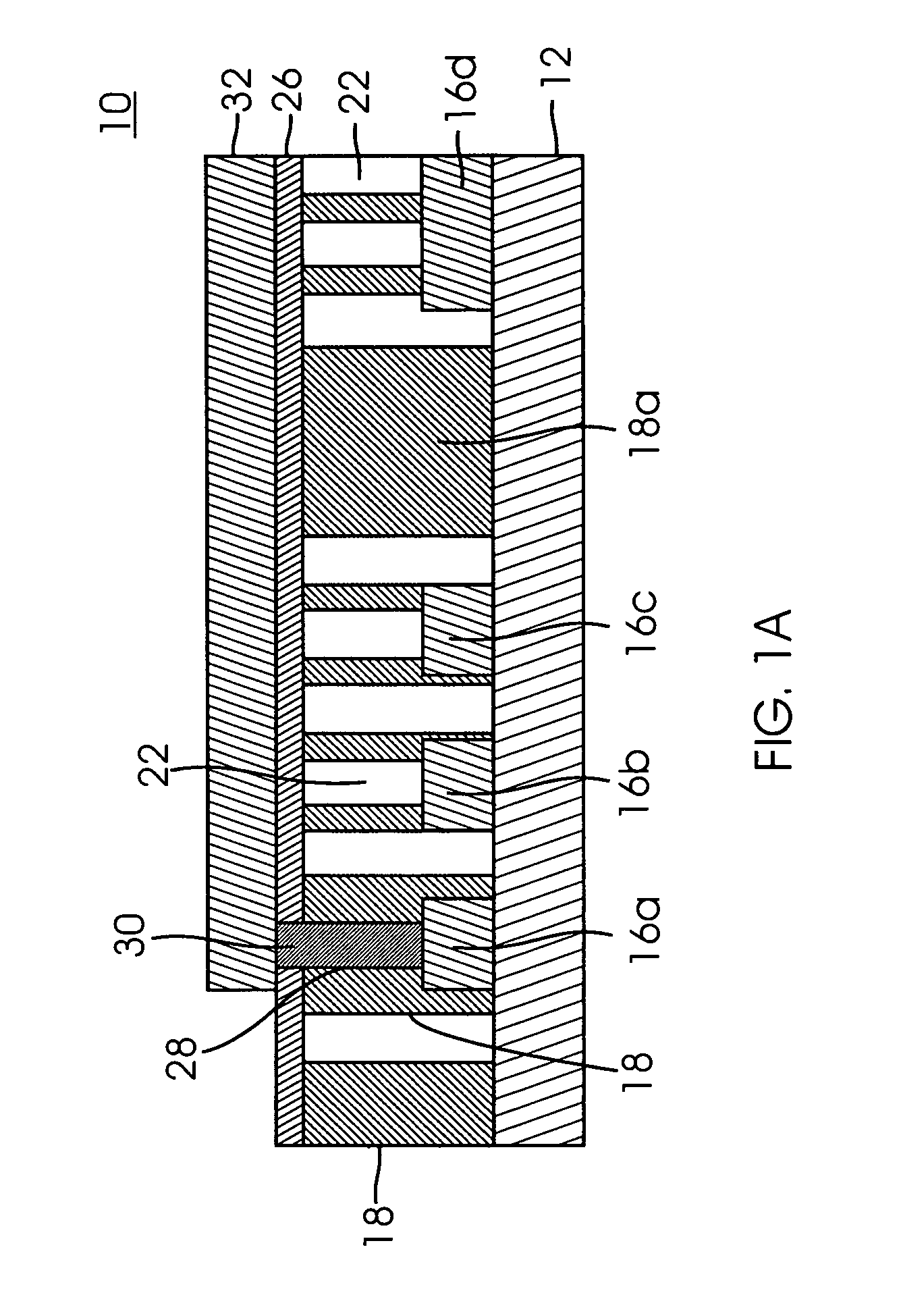
[0034]FIG. 1A is a vertical cross sectional view of a novel interconnect structure 10 formed on a layer 12 according to the present invention. Layer 12 can be a semiconductor substrate formed from a semiconductor material, such as silicon or gallium arsenide (GaAs), or a dielectric layer formed from an insulative material. When layer 12 is a substrate, layer 12 can include transistors, diodes, and other semiconductor devices that are well known in the art. When layer 12 is a dielectric layer, layer 12 can contain vias or contacts (not shown) for providing an electrical connection between interconnect lines 16 and lower structures (not shown) of the integrated circuits.

[0035]A first conductive layer 16 is deposited over layer 12 and patterned to form interconnect lines 16a–16d. A patterned conductive layer is referred to also as an interconnect layer. After the first conductive layer 16 is patterned, a plurality of interconnect lines 16, separated by spaces 17 (see FIG. 2), remain. T...

fourth embodiment

[0064]FIGS. 19–33 are cross-sectional views of an interconnect structure according to the present invention at selected stages of fabrication. This embodiment utilizes another dielectric layer (i.e., a second dielectric layer 62C) in addition to the first dielectric layer 18C. This embodiment provides an interconnect that can have two different dielectric materials. For example, one dielectric layer can be made from SiO2, and the second dielectric layer can be made from a low-k material.

second embodiment

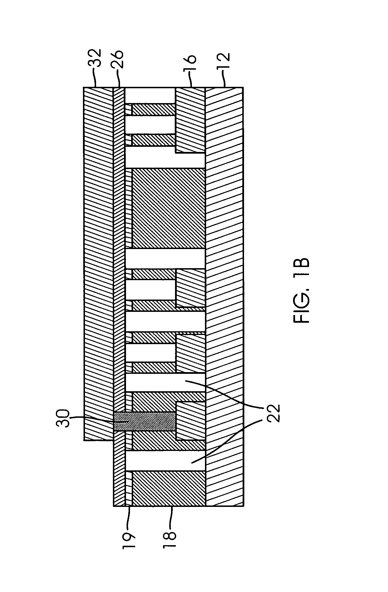
[0065]This embodiment is based on FIG. 17 since only intra-line capacitance is addressed. However, the steps in FIGS. 19–25 correspond generally to those in FIGS. 2, 3A–3C, 4–6, respectively, and description related thereto will not be repeated herein. The main difference in this embodiment is that a second dielectric layer 62C is deposited over sealing layer 26C in FIG. 26, and the processing thereafter (such as via hole formation) affects second dielectric layer 62C. Moreover, the steps in FIGS. 27 and 28 correspond generally to those in FIGS. 7 and 8, respectively, except that photoresist is applied to second dielectric layer 62C instead of sealing layer 26, and the via hole is etched in second dielectric layer 62C in addition to sealing layer 26C and first dielectric layer 18C.

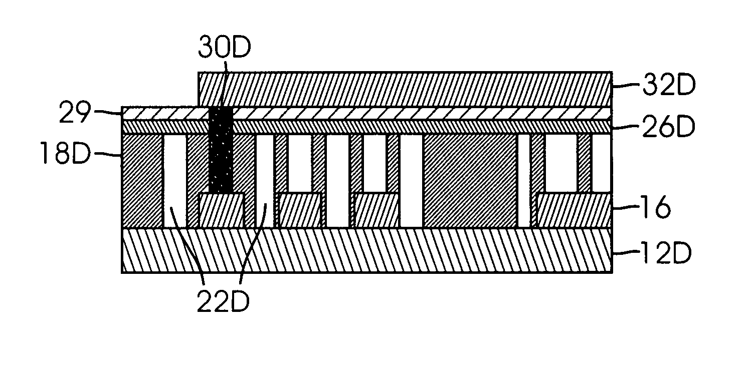
[0066]FIG. 31B illustrates the interconnect structure of the fourth embodiment having hard masks 19C and 19D. If first dielectric layer 18C and second dielectric layer 62C (described below) are made with a...


PUM


Abstract

An interconnect structure and fabrication method are provided to form air gaps between interconnect lines and between interconnect layers. A conductive material is deposited and patterned to form a first level of interconnect lines. A first dielectric layer is deposited over the first level of interconnect lines. One or more air gaps are formed in the first dielectric layer to reduce inter-layer capacitance, intra-layer capacitance or both inter-layer and intra-layer capacitance. At least one support pillar remains in the first dielectric layer to promote mechanical strength and thermal conductivity. A sealing layer is deposited over the first insulative layer to seal the air gaps. Via holes are patterned and etched through the sealing layer and the first dielectric layer. A conductive material is deposited to fill the via holes and form conductive plugs therein. Thereafter, a conductive material is deposited and patterned to form a second level of interconnect lines.

Description

REFERENCE TO RELATED DOCUMENTS[0001]This application is a divisional application of U.S. patent application Ser. No. 09 / 193,499, filed Nov. 16, 1998 now U.S. Pat. No. 6,211,561 and entitled “INTERCONNECT STRUCTURE AND METHOD EMPLOYING AIR GAPS BETWEEN METAL LINES AND BETWEEN METAL LAYERS.”FIELD OF THE INVENTION[0002]The present invention relates generally to semiconductor processing. More specifically, this invention relates to a novel interconnect structure and method for forming integrated circuits having air gaps between interconnect lines and between interconnect layers.BACKGROUND OF THE INVENTION[0003]Those involved with the manufacture of high performance ultra-large scale integration (ULSI) integrated circuits must address and be sensitive to RC delay problems, cross-talk issues, and power dissipation.[0004]RC delay is the propagation delay of a signal caused by resistance in metal lines and the capacitance between metal lines and between metal layers. RC delay is undesirable...

Claims


Application Information

Patent Timeline
IPC IPC(8): H01L21/4763H01L21/768H01L23/482H01L23/522H01L23/532
CPCH01L21/7682H01L23/4821H01L23/5222H01L23/5329H01L2924/0002H01L2924/00
Inventor ZHAO, BIN
Owner NEWPORT FAB
Why Eureka
Try Eureka