Electro-optic array interface

a technology of array interface and array array, applied in the direction of static indicating device, material analysis by optical means, instruments, etc., can solve the problems of ghz range performance that cannot be fully exploited, constraint that will become increasingly severe, and the challenge of routing signals off-chip and into the system in the ghz frequency range is expected to exceed the performance of on-chip performance, and achieve high interconnect density

Inactive Publication Date: 2006-06-06
CIENCIA
View PDF13 Cites 19 Cited by
  • Summary
  • Abstract
  • Description
  • Claims
  • Application Information

AI Technical Summary

Problems solved by technology

Performance in the GHz range can only be fully exploited if the off-chip interconnection technology provides appropriate bandwidth, a constraint that will become increasingly more severe during the next ten years.
This means that the challenge of routing signals off-chip and into the system in the GHz frequency range is expected to exceed that of achieving on-chip performance at these frequencies.
In addition, highly parallel, next-generation computational systems will require highly dense connection networks containing many long-distance connections.
In such highly connected, highly parallel systems, the module-to-module and long distance chip-to-chip connections are responsible for the majority of the power dissipation, time delay and surface area.
The density and total number of these interconnections has become a major challenge due to physical space requirements and to interfering cross talk.
It is clear, that an optical processing format could help significantly with these interconnections, but such help can not be applied until appropriate electro optic interfaces are available.
These are limited in the number of practical connections that can be implemented.
Optical information processing can perform a multitude of operations because of its complex amplitude processing capability using several dimensions.
Both approaches have trade-offs, and difficulties with signal to noise, which have brought forward many versions of distortion invariant matched filters.
However, the prevalent electronic digital computing offers much greater flexibility for various implementations, and will not soon give way to an all-optical approach.
As integrated circuits (and modules) have grown in complexity and size, the number of in-out interconnections has become almost impossible to implement.
The fundamental problem is that there is simply no surface area available for more electrical conductors.
There is an adverse effect on power, speed, and heat.
Although desirable for some emerging systems, it is extremely difficult to make the parallelism dynamically reconfigurable, and crosstalk can be a problem, especially if any analog signals are present.
Special crystals are prohibitively expensive and cumbersome to work with, but can be fast (GHz).
To date, these materials suffer from drive level and lifetime problems.

Method used


Image

  • Electro-optic array interface
  • Electro-optic array interface
  • Electro-optic array interface

Examples


Embodiment Construction

1.2.1 Surface Plasmon Resonance

[0029]At the heart of the SPROM is the high-density, dynamically reconfigurable reflector microarray. Since its function is based on grating-coupled SPR, understanding its operation and fabrication require some knowledge of the physics of SPR, which we briefly review in this section.

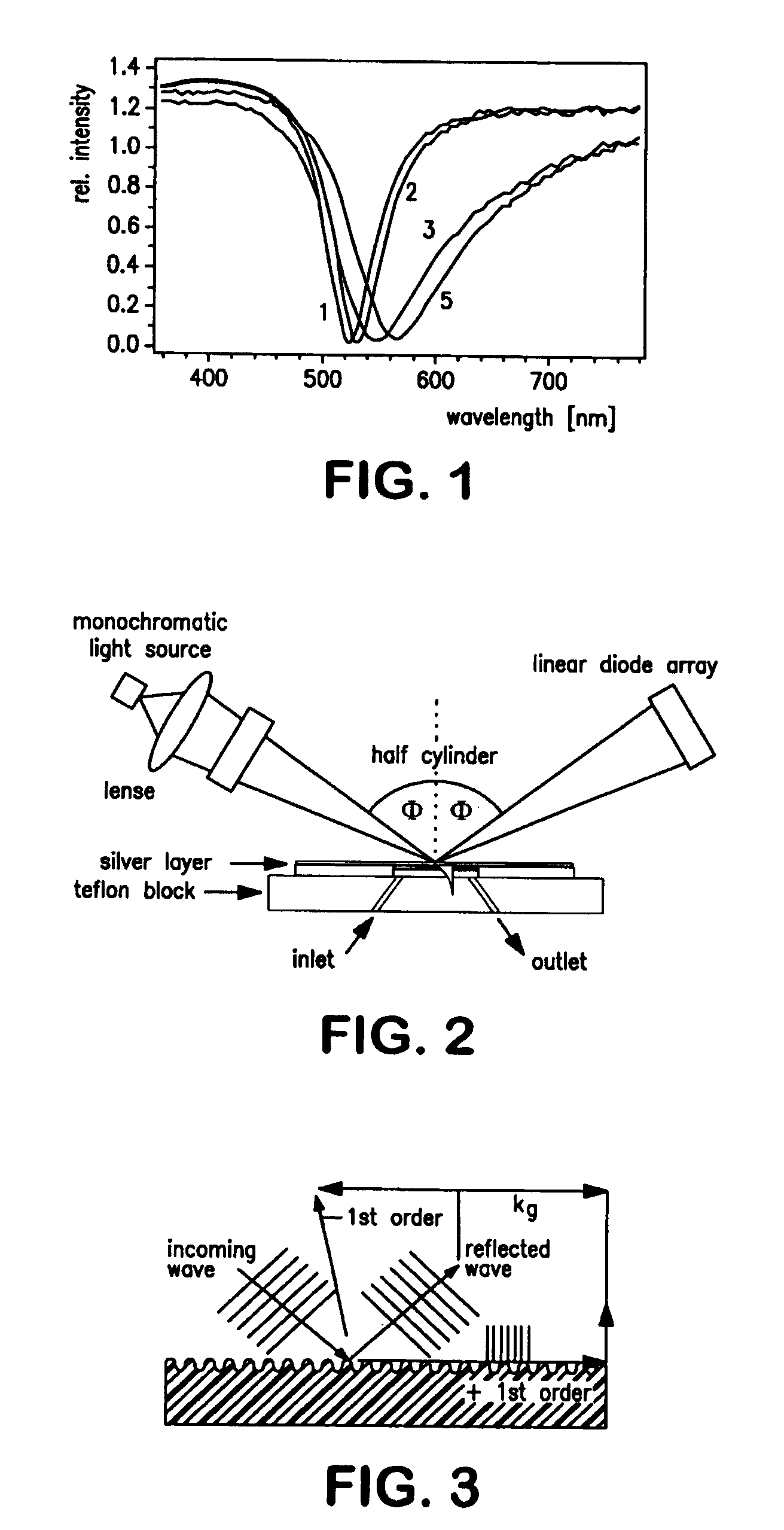
[0030]The theory of surface plasmon resonance is well established. When a metal surface is illuminated by TM-polarized light of the appropriate wavelength and angle of incidence, a resonance condition occurs and energy from the light is coupled into the electrons of the metal to excite what is called a surface plasmon. A surface plasmon is a propagating electron oscillation in a metal at a metal / dielectric interface. The associated electromagnetic fields constitute a guided surface mode of the conductor-dielectric interface and are evanescent in each medium with intensity decaying exponentially away from the surface. Penetration into the dielectric depends on the wavelength...


PUM

PropertyMeasurementUnit
widthaaaaaaaaaa
on-chip clock frequenciesaaaaaaaaaa

Abstract

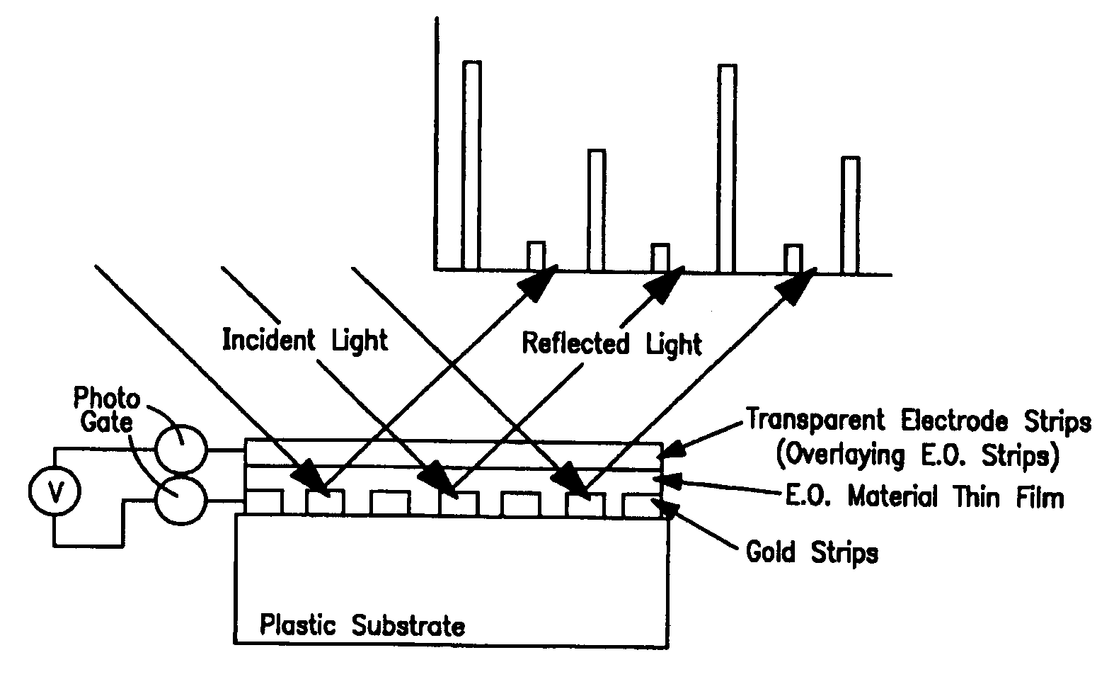
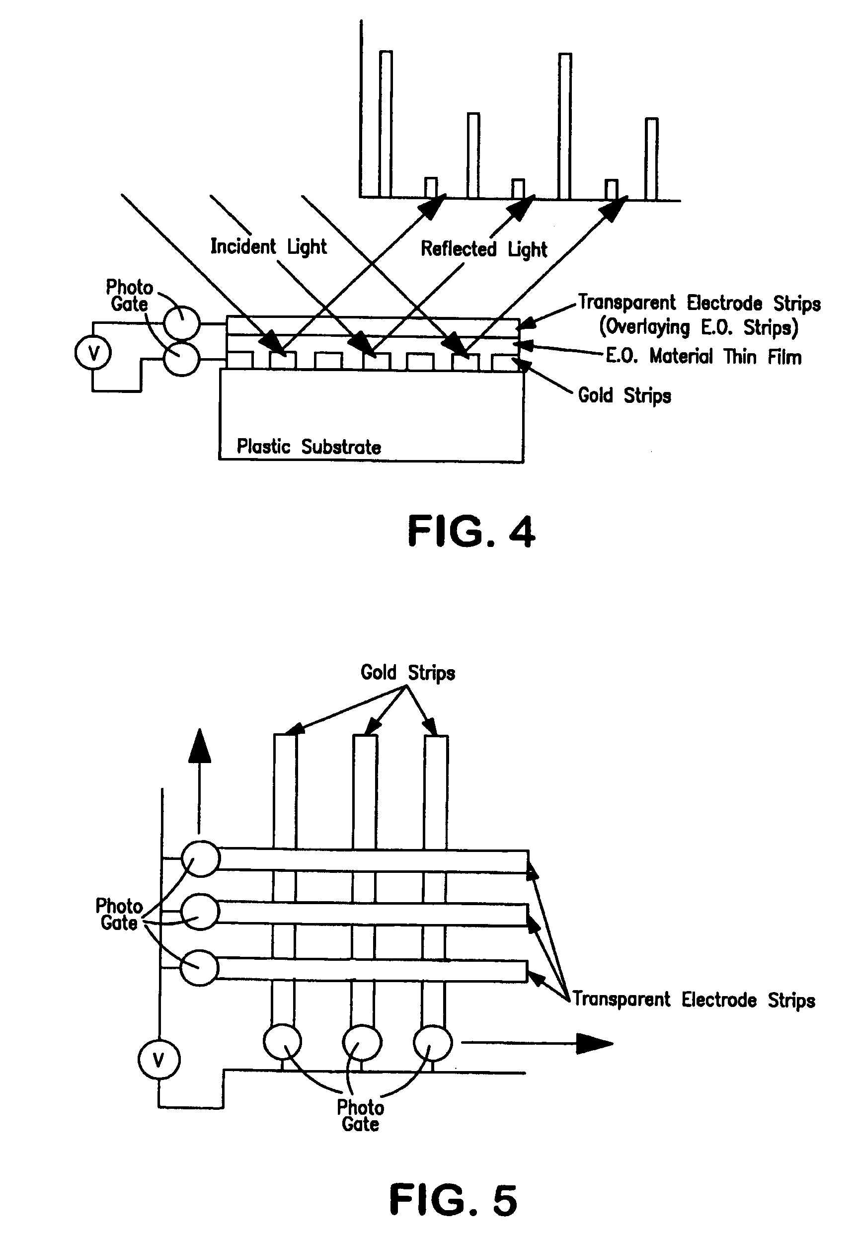
A grating coupled surface plasmon resonance optical modulator is disclosed. A electro-optic polymer dielectric is deposited on the metallic surface of a diffraction grating to provide a metal / dielectric interface. A surface plasmon will propagate at the metal / dielectric interface in a resonant condition, e.g., when the metal surface is illuminated by transverse magnetic (TM) polarized light of the appropriate wavelength, angle of incidence and phase velocity. In the present invention, phase velocity is controlled by the diffraction grating. A transparent electrode deposited on the electro-optic layer allows an electrical potential to be applied across the electro-optic polymer. The applied electrical potential (voltage) changes the index of refraction of the electro-optic polymer, thereby disrupting the resonant condition to produce an optically detectable change in reflectance of incident light from the metal layer. The disclosed grating coupled surface plasmon resonance optical modulator may be configured as an electronically or optically addressable array.

Description

[0001]The proposed invention relates generally to the field of spatial light modulators and optical interconnects. The invention is an optically addressable, dynamically reconfigurable, bi-directional, high-density, optical interconnect microarray based on the phenomenon of grating-coupled surface plasmon resonance (GCSPR). The device addresses the need for dense, fast, low power dissipation interconnect technology created by highly parallel, next generation computational systems. It will be able to provide connections between chips within a given module or between chips located on different modules with interconnection densities (number of microarray elements, N, per unit area) of the order of tens of thousands per cm2 while reaching modulation or switch rates of the order of tens of GHz.BACKGROUND OF THE INVENTION[0002]At present, microprocessors are providing on-chip clock frequencies on the order of 1 GHz. The International Technology Roadmap for Semiconductors (ITRS) forecasts ...

Claims


Application Information

Patent Timeline
Patent Type & Authority Patents(United States)
IPC IPC(8): G02F1/03G02B26/00G02B5/18G02F1/00G09G3/36G02B6/10G02B6/122G02F1/061G02F1/07
CPCB82Y20/00G02B6/1226G02F1/061G02F2203/10G02F2201/307
Inventor SAWIN, RAYFERNANDEZ, SALVADOR M.
Owner CIENCIA
Why Eureka
Try Eureka