Circuit substrate and fabrication method thereof

a technology of circuit substrate and fabrication method, which is applied in the field of circuit substrate, can solve the problems of complex landless design process, increased cost, and difficulty in fabricating circuit substrate, and achieve the effects of reducing the number of vias, reducing the bent portions of conductive traces, and increasing the density of conductive traces

Active Publication Date: 2006-06-13
ADVANCED SEMICON ENG INC
View PDF3 Cites 22 Cited by
  • Summary
  • Abstract
  • Description
  • Claims
  • Application Information

AI Technical Summary

Benefits of technology

[0012]Circuit substrate of this invention is formed by filling an insulator in the via and the cutting street so that the metal layer formed on the inner wall of the via is separated into a plurality of separated metal layers. In such a manner, the separated metal layers in the via are electrically isolated from each other. In other words, each separated metal layers in the same via can be provided to electrically connect its corresponding conductive traces layer. Consequently, the number of the vias will be reduced so as to increase the density of the conductive traces layout. Besides, it can also reduce the bent portions of the conductive traces so as to reduce the distance of signal transmission.
[0013]Moreover, this invention further discloses a fabrication method of the circuit substrate as mentioned above. The method includes the steps of forming a metal layer on the inner wall of the via, cutting the via to form at least one cutting street to separate the metal layer into a plurality of separated metal layers. In such a manner, the via can be separated into a plurality of separated vias. Consequently, not only this process can simplify the process of plating metal layers on the inner wall of smaller via, but also speed up the formation for large amount of the vias.

Problems solved by technology

However, the process of the landless design is complex and the cost is increased.
Consequently, it will be difficult to fabricate the circuit substrate.
Besides, the quality of the electricity will be seriously affected in that, with reference to FIG. 2, the bent portions of the conductive traces and the distance of the signal transmission are increased.

Method used


Image

  • Circuit substrate and fabrication method thereof
  • Circuit substrate and fabrication method thereof
  • Circuit substrate and fabrication method thereof

Examples


Embodiment Construction

[0022]The circuit substrate and fabrication method thereof according to the preferred embodiment of this invention will be described herein below with reference to the accompanying drawings, wherein the same reference numbers refer to the same elements.

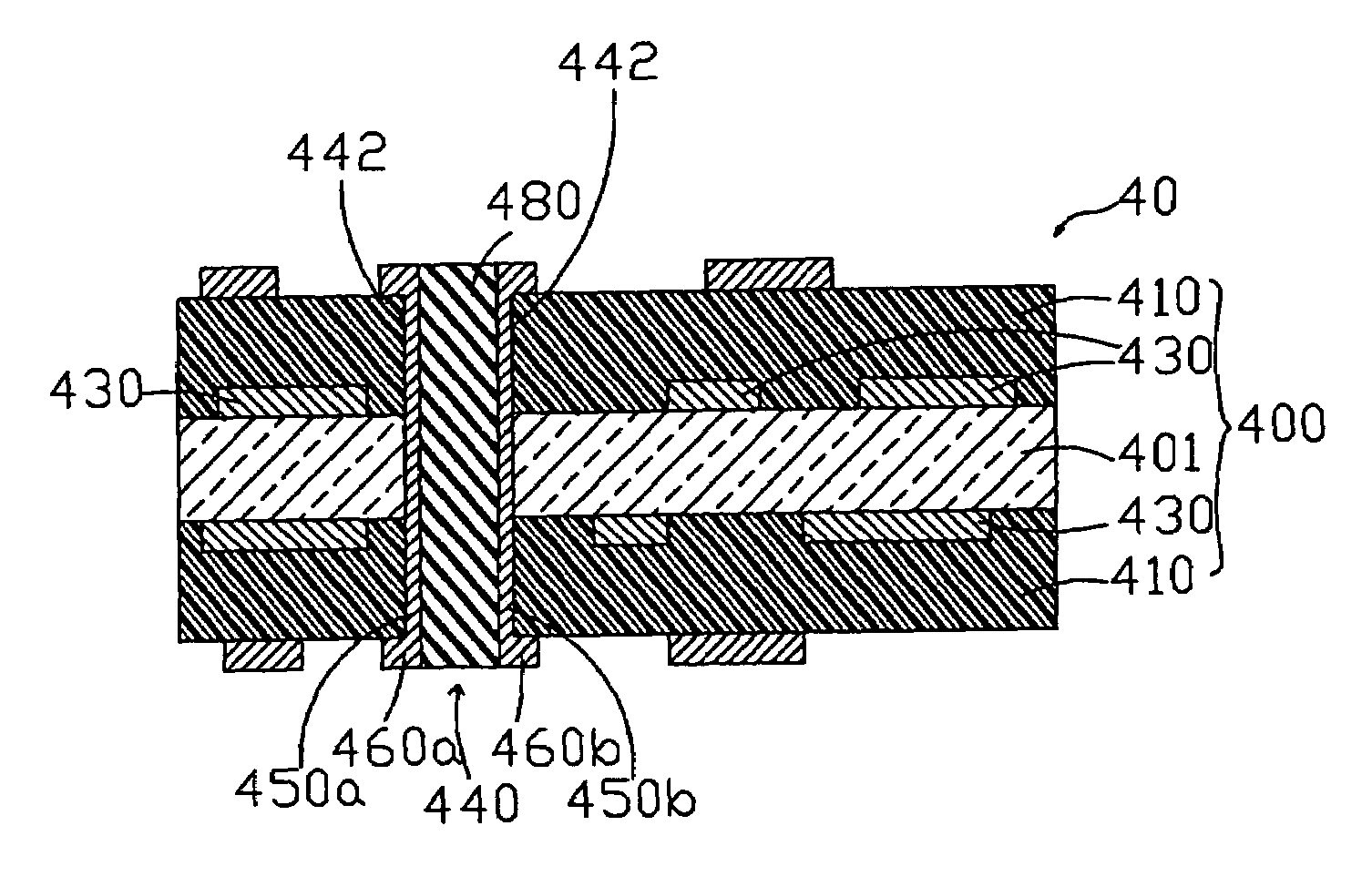
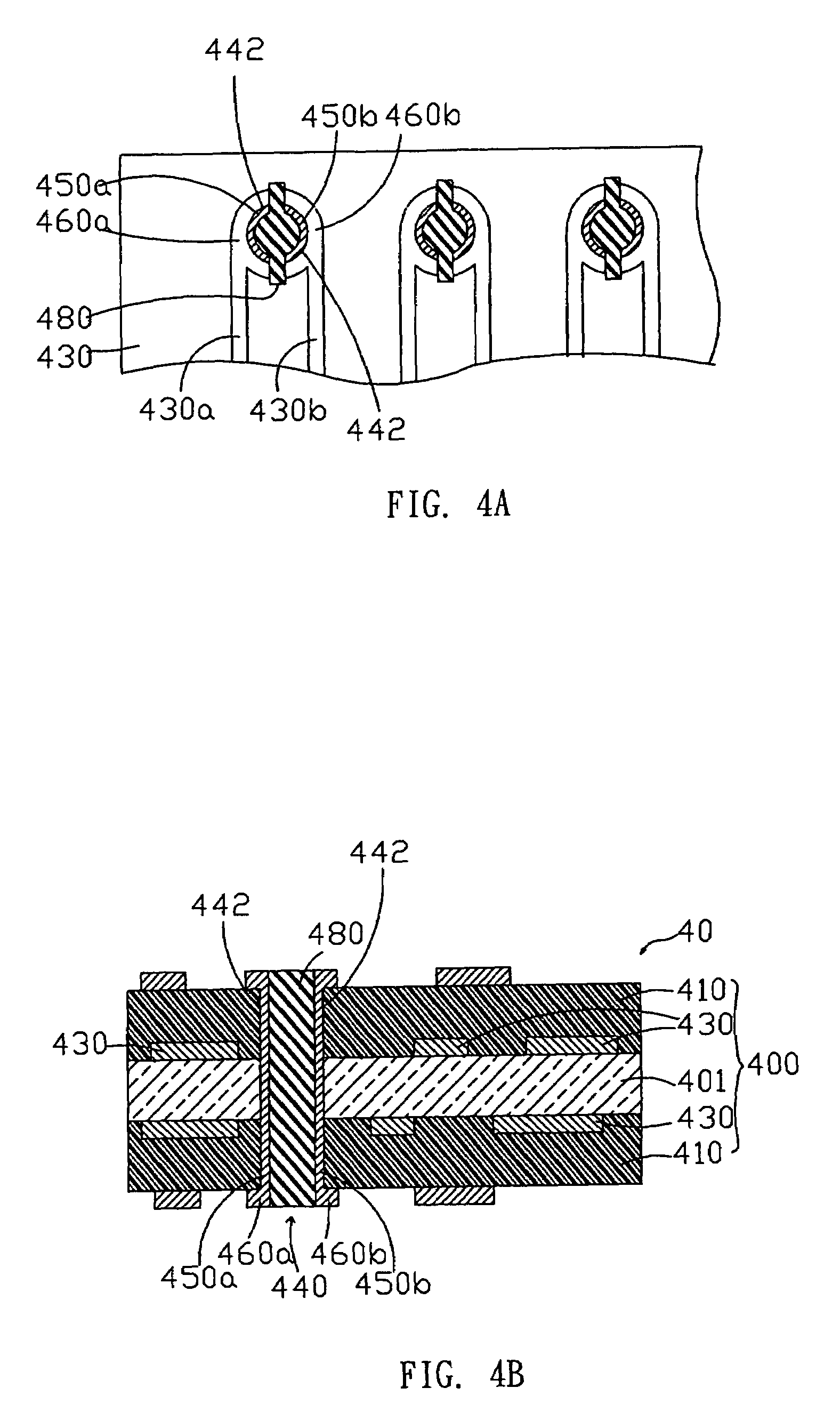
[0023]In accordance with a preferred embodiment as shown in FIGS. 4A and 4B, a circuit substrate 40 includes a board 400, a via 440, metal layers 450a and 450b, and an insulator 480. The board 400 comprises a core board 401, and a plurality of insulating layers 410 and conductive traces layers 430 wherein the insulating layers 410 and the conductive traces layers 430 are interlaced with each other. The material of the insulating layers 410 can be Bismaleimide-Triazine (BT), glass epoxy resins (FR4), epoxy or polyimide. The conductive traces layer 430 can be formed by the steps of forming a copper foil on the surface of the insulating layer 401, forming a patterned photo-resist layer on the copper foil, removing a portion of the copper...


PUM

PropertyMeasurementUnit
diameteraaaaaaaaaa
diameteraaaaaaaaaa
thicknessaaaaaaaaaa

Abstract

A circuit substrate includes a board, a plurality of metal layers and an insulator. The board has a plurality of conductive traces layers and a via formed therein. The metal layers are formed on the inner wall of the via and each of the metal layers is electrically connected to its corresponding conductive traces layer. The via is filled with the insulator so that each of the metal layers is electrically isolated from each other. In addition, this invention also provides a fabrication method of the circuit substrate.

Description

BACKGROUND OF THE INVENTION[0001]1. Field of Invention[0002]This invention relates to a circuit substrate and a fabrication method thereof. More particularly, the present invention is directed to a circuit substrate, suitable for an integrated circuit, and fabrication method thereof.[0003]2. Related Art[0004]Presently, circuit substrate is commonly employed as carrier in electrical industry. Not only circuit substrate is employed as printed circuit board (PCB) but also package substrate, which is applicable to an integrated circuit package. Recently, a high-density circuit substrate having multiple layers and conductive traces with fine pitches is improved for the integration of the integrated circuits (ICs), and the need of thinner ICs package and higher input / output counts.[0005]As shown in FIG. 1, a circuit substrate 10 mainly includes a board 100. The board 100 comprises a core board 101, a plurality of insulating layers 110 and conductive traces layers 130. The insulating layer...

Claims


Application Information

Patent Timeline
Patent Type & Authority Patents(United States)
IPC IPC(8): H01L21/20H01L21/36H05K3/28H01L23/498H05K1/11H05K3/04H05K3/40H05K3/42H05K3/46
CPCH01L23/49827H05K1/115H05K3/403H05K3/043H05K3/429H05K2201/09509H01L2924/0002H05K2201/09536H05K2201/0959H05K2201/09645H01L2924/00
Inventor OU, IN-DEHUNG, CHIH-PINCHEN, CHIA-SHANGLIN, KUANG-HUACHAO, SHIN-HUA
Owner ADVANCED SEMICON ENG INC
Why Eureka
Try Eureka