Contamination prevention in optical system

a technology of optical system and contamination prevention, applied in the field of optical structure, can solve the problems of difficult to completely remove impurity gases, difficult to separate only the light path from the surrounding ambience, and difficult to purge the entire path of exposure light, so as to prevent adhesion of depositions, prevent contamination of optical elements, and keep the surface clean

Inactive Publication Date: 2006-06-13
CANON KK
View PDF21 Cites 51 Cited by
  • Summary
  • Abstract
  • Description
  • Claims
  • Application Information

AI Technical Summary

Benefits of technology

[0008]It is accordingly an object of the present invention to provide an optical structure and / or a method of preventing contamination of the same, in which a clean gas is supplied efficiently to the surface, or in the neighborhood thereof, of an optical element being isolated from a surrounding ambience, thereby to keep the surface clean and to prevent adhesion of depositions thereon. This assures minimization of the influence of the gas flow to the imaging performance and adjustment of the imaging position, for example, such that contamination of the optical element can be prevented with a very small amount of gas flow.

Problems solved by technology

For these reasons, it is very difficult to completely remove impurity gases which cause depositions.
However, it is practically difficult to purge the entire path of exposure light.
Therefore, it is difficult to separate only the light path from the surrounding ambience and to purge the same.
This leads to degradation of the optical performance, such as a decrease of illuminance, for example, and thus it causes a necessity of periodic washing or replacement.
Here, in exposure apparatuses, any fluctuation in an ambience is adversely influential to the imaging performance.
It is, therefore, very difficult to decrease the impurity concentration at the lens surface effectively.
In these methods, a gas product from a wafer is rather conveyed to the lens surface, along the gas flow, such that sufficient contamination prevention is not attainable.
This method has paid particular note to an oxygen concentration in the space from the projection optical system to the wafer, but the efficiency itself regarding contamination prevention at the bottom face of the projection optical system is not so good.
Any change in temperature or pressure of an ambience in the space through which the measurement light passes leads to a measurement error, and this applies a large influence to the position adjustment for the wafer imaging position.
For these reasons, the flow of a gas of a large flow rate or any fluctuation in pressure or temperature causes an error of the wafer position adjustment and degradation of the imaging performance.

Method used


Image

  • Contamination prevention in optical system
  • Contamination prevention in optical system
  • Contamination prevention in optical system

Examples


embodiment 1

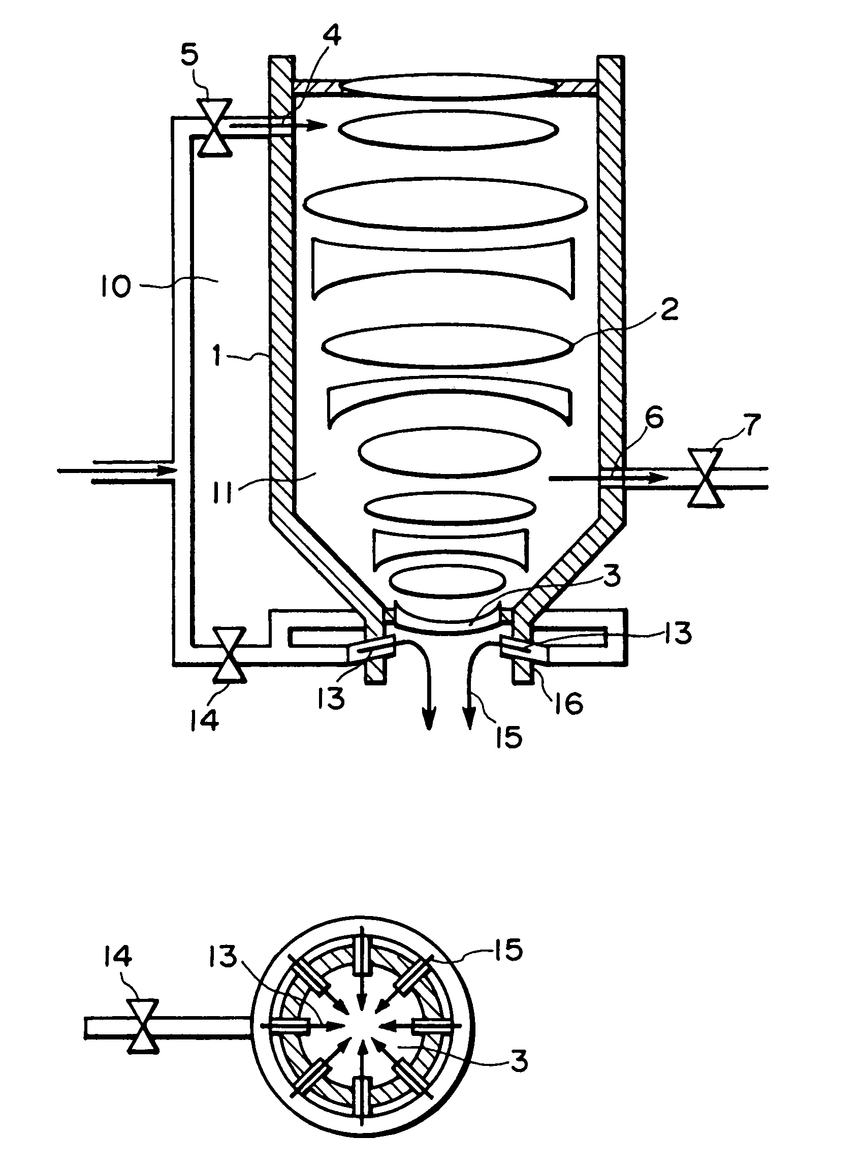
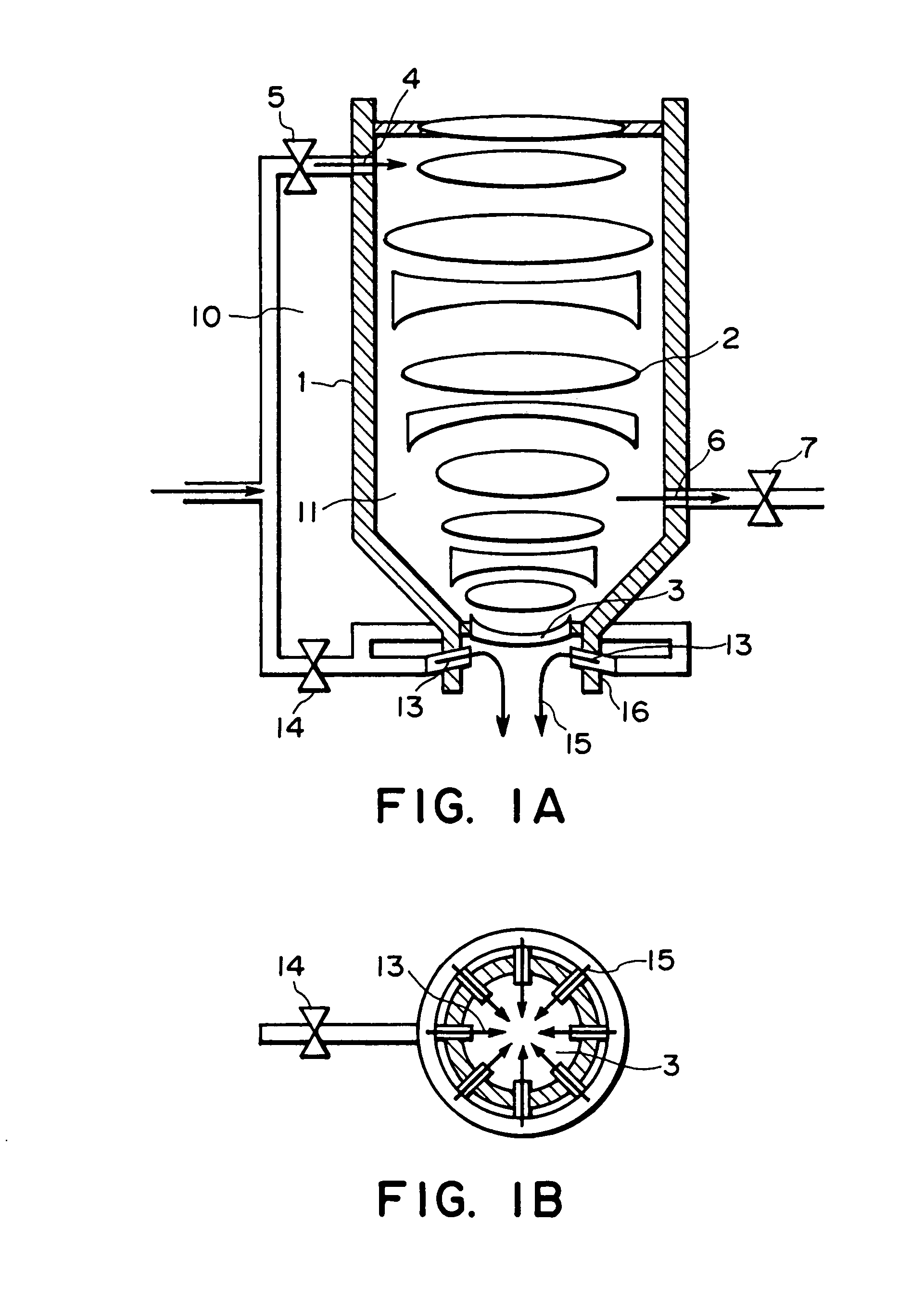
[0066]FIGS. 1A and 1B are schematic views of a first embodiment of the present invention. This is a typical example of the present invention as applied to a bottom lens of a projection system in a semiconductor exposure apparatus. FIG. 1A is a schematic and sectional view of a projection barrel and FIG. 1B is a schematic view of the bottom of the barrel.

[0067]As shown in FIG. 1A, the projection system of the semiconductor exposure apparatus comprises a plurality of lenses 2. The whole optical system is accommodated in a barrel 1 which is closed (and purged) so that an ambient gas in a chamber ambience enters into the barrel. Along the light path, the top of the projection system, that is, the lens closest to a reticle, and the bottom of the projection lens, that is, the lens 3 closest to a wafer, serve to intercept the ambience.

[0068]The barrel is provided with a gas supply port 4 and a gas discharging port 6 so that a clean gas without containing impurities can be supplied to the i...

embodiment 2

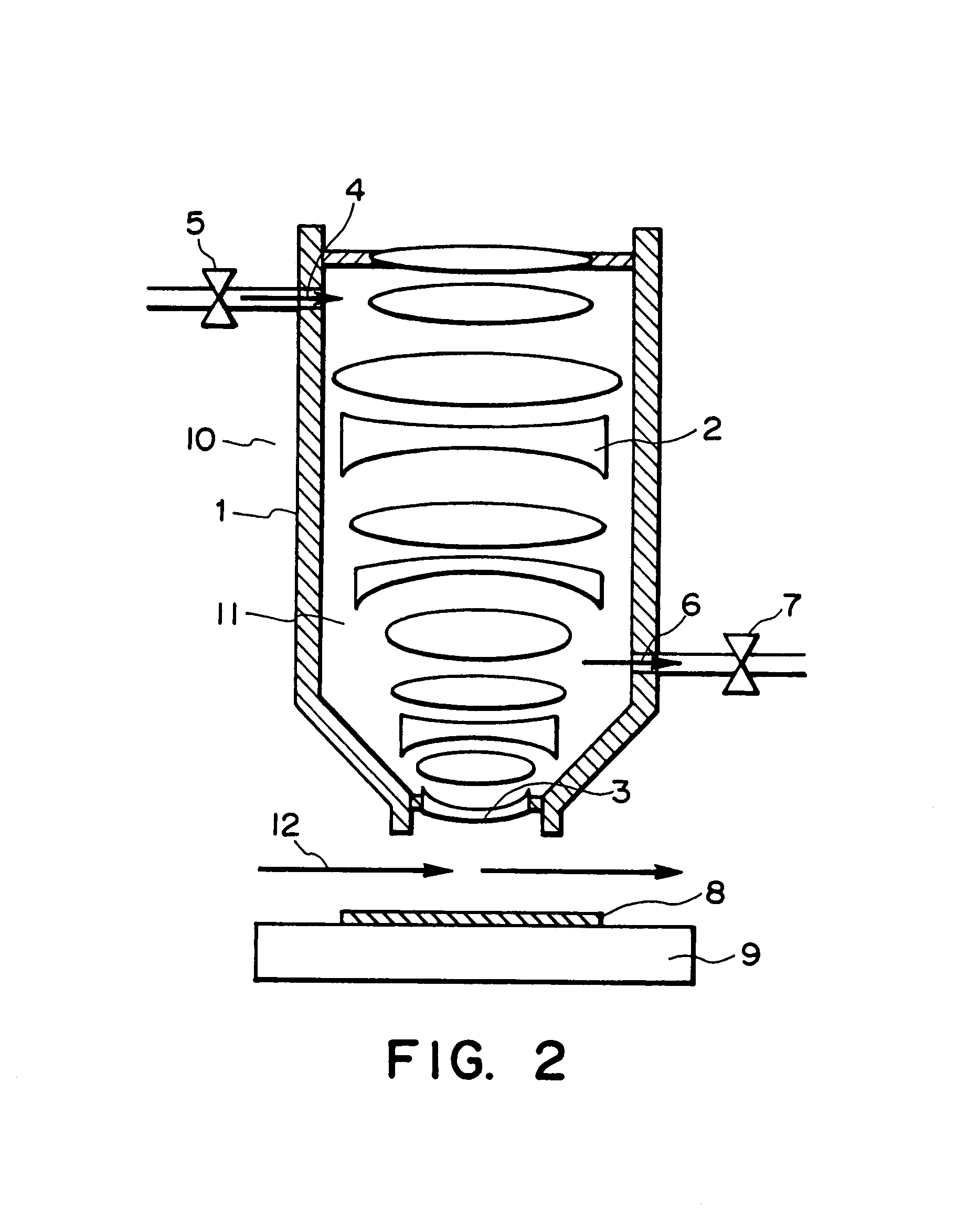
[0078]FIG. 4 is a schematic view of a second embodiment of the present invention. In the gas supplying method of the first embodiment, there may be cases wherein, depending on the size or shape of the lens, for example, the gas that flows form the lens to the wafer surface is diffused of a resist gas. In consideration of it, as shown in FIG. 4, a gas discharging port 17 may be provided below the supply port. This is effective to produce a gas flow.

[0079]Also, in this case, there may be a plurality of gas discharging ports disposed revolutionally symmetrically with respect to the optical axis, like the gas supply ports.

[0080]Further, the shape and position of these gas supply ports and gas discharging ports should be determined so that the gas flows appropriately. Moreover, the gas supplying pressure and flow rate as well as the gas discharging pressure from the gas discharging port should be adjusted appropriately. The pressure inside the projection barrel is maintained constant, an...

embodiment 3

[0081]FIGS. 5A and 5B are schematic views of a third embodiment of the present invention, wherein FIG. 5A is a schematic and sectional view of a projection system lens barrel and FIG. 5B is a schematic view of the lens bottom face.

[0082]A gas supply port 18 and a gas discharging port 20 are provided in the neighborhood of the bottom-most lens of the projection system, that is, the lens 3 closest to the wafer, and the lens surface of the barrel 22 at the top of the projection system, facing the chamber ambience side, such that a clean gas is caused to flow. As shown in FIG. 5B, the gas supply port 18 is provided at one of lens side faces while the gas discharging port 20 is provided at the opposite lens side face, by which an effective gas flow is produced locally upon the lens surface. Particularly, plural gas supply ports and plural gas discharging ports may preferably be provided. On that occasion, a gas flows uniformly along the lens surface.

[0083]Further, in accordance with the ...


PUM

PropertyMeasurementUnit
wavelengthaaaaaaaaaa
wavelengthsaaaaaaaaaa

Abstract

An exposure apparatus for illuminating a pattern with light from a light source and for exposing a predetermined surface with light from the pattern includes (i) a projection optical system for projecting the pattern onto the predetermined surface, the projection optical system having at least one optical element having optical surfaces, and (ii) a gas supplying device for locally supplying a gas to the at least one optical element. In one aspect, the gas supplying device directly blows the gas toward one of the optical surfaces of the at least one optical element, which is closest to the predetermined surface, from the predetermined surface side.

Description

FIELD OF THE INVENTION AND RELATED ART[0001]This invention relates to an optical structure and a method of preventing contamination of an optical structure. More particularly, the invention concerns a technology suitably usable in an optical structure, particularly, a semiconductor exposure apparatus, for example, which uses a wavelength of light in an ultraviolet region as a light source, for effectively preventing contamination of a surface of an optical element isolated from a surrounding ambience, the surface being at the ambience side.[0002]Semiconductor integrated circuits have become more and more miniaturized year after year, and, in order to meet this, exposure apparatuses for transferring a circuit pattern onto a wafer are required to have a performance capable of transferring a finer pattern. Thus, the wavelength of exposure light used in such exposure apparatuses becomes shorter and shorter. Currently, i-line (wavelength 365 nm) or KrF excimer laser light (wavelength 245...

Claims


Application Information

Patent Timeline
Patent Type & Authority Patents(United States)
IPC IPC(8): G03B27/52G03B27/54G03F7/20H01L21/027
CPCG03F7/70883G03F7/70933G03F7/70916
Inventor TSUKAMOTO, MASAMI
Owner CANON KK
Why Eureka
Try Eureka