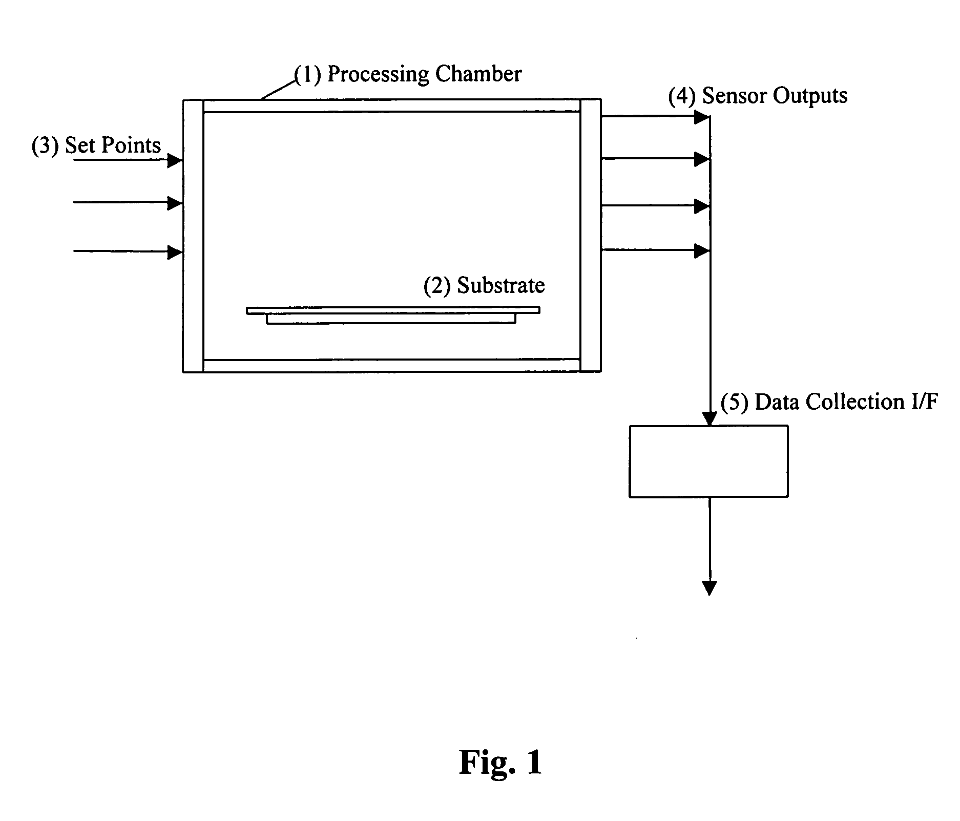
A typical semiconductor manufacturing
plant (or fab) can require several hundred highly complex tools to fabricate intricate devices such as microprocessors or memory chips on a
silicon substrate or wafer.
Faults can and do occur on these manufacturing tools.
A fault on a single wafer can compromise all devices on that wafer and all subsequent steps on that wafer may be worthless and the wafer scrapped.
The manufacturing tools are complex and many different faults can occur, some specific to the tool process being run at the time, that
impact tool productivity and yield (in the case of a
plasma chamber, the process being run at any given time is known in the art as the “
recipe”).
If there is a deviation in any of the process parameters, then the quality of the output may be negatively impacted.
Another type of fault concerns excursions in the process itself.
This control technique has a number of limitations.
The first problem is that monitoring all SPC charts is not scalable, since there can be ten's of sensors per tool and several hundred tools in the fab.
This is because the
processing tools are typically complex and their output depends on their combined inputs as well as the conditions of the tool itself.
This is known to be a very expensive approach to
process control, since running test wafers and halting real production to test
process quality negatively impacts factory yield and productivity.
The third problem relates to the difficulty of setting SPC limits on the tool sensors.
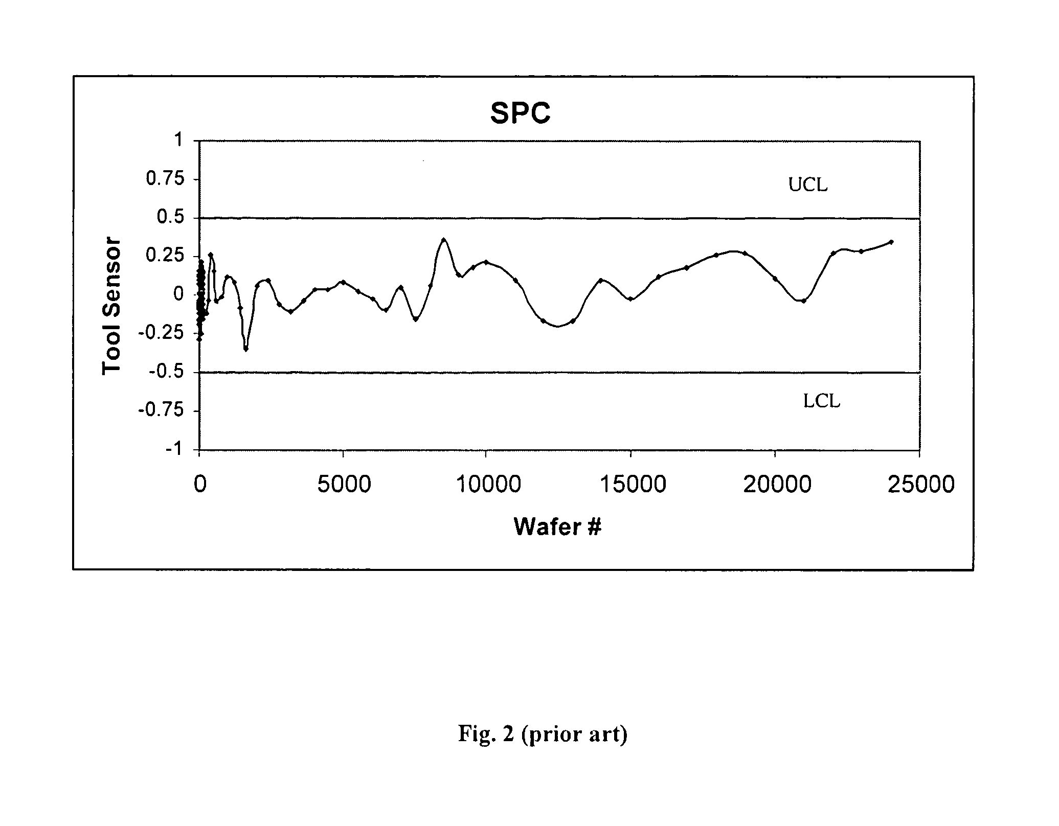
It will also be seen that the data is highly non-normal, with auto-correlation and discontinuities.
The SPC approach therefore cannot
handle this data effectively and significant events can be lost in the data.
Indeed, in the example of FIG. 3, the fault which occurred at wafer 1018 is impossible to pick out of the data using the SPC approach.
However, since the multivarate approach is statistically based, the third problem is not addressed.
However, this single multivariate statistic reports a couple of statistical excursions with greater than 99% confidence because they deviate from statistically
normal behaviour, but misses the real fault condition.
The magnitude of the excursion is difficult to interpret, again because it is statistically based.
A further issue arises when using the statistical approach in a multi-tool semiconductor manufacturing site.
Therefore, a statistical fault detection model cannot be transferred from one chamber to another, as small differences in sensor response would trigger a
false alarm.
This is a further limitation in the approach.
However, the reliance on accurate determination of, in this case, CD, or in the general case, a
process quality metric, makes the technique very expensive to operate.
One problem with this approach is that the process output depends on several inputs and unless all are controlled, the process output cannot be inferred.
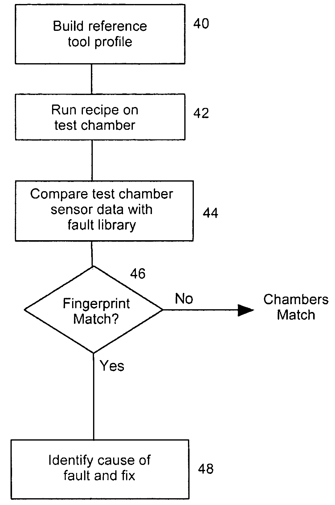
A separate but related problem is that of tool matching.
However, as discussed, differences between outwardly similar chambers can and do occur, resulting in a mis-matched output set.
This mis-match ultimately impacts factory productivity and yield.
Firstly, every attempt is made to design processes with wide operation windows so that small chamber-to-chamber differences have a negligible effect on the process output.
Secondly, large differences in chamber output are tolerated by device sorting according to final specification; for example, speed binning in the case of micro-processor manufacturing.
Thirdly, every attempt is made to make all chambers the same.
This can involve trial-and-error parts swapping as well as extensive calibration checks and it is generally a laborious approach.
Device specification sorting is expensive as below par devices have much lower market value.
Finally, the effort to make all chambers the same by trial-and-error parts swapping and calibration checks is a diminishing returns equation, since in many cases great time and effort can be spent on the problem.
These quality checks are generally ex-situ and a time
delay is inevitable between
processing a set of wafers and knowing if the output differences will
impact yield.
The problem with using the raw sensor data to determine (a) above is that it is confounded by (b) and (c).
As stated above, the approach is often trial-and-error, involving parts swap-out and calibration until the chamber outputs are matched.
This approach makes no effort to solve chamber mis-matches and badly matched chambers would be used as little as possible.
However, the variance as viewed in PCA space remains a
confounding of real (output-impacting) chamber differences, benign chamber differences and sensor set differences.

