Semiconductor leadframes plated with thick nickel, minimum palladium, and pure tin

a technology of nickel-plated leadframes and semiconductors, applied in the field of semiconductor leadframes plated with minimum palladium, thin nickel, pure tin, etc., can solve the problems of inability to achieve fine-pitch devices

Inactive Publication Date: 2006-06-20
TEXAS INSTR INC
View PDF14 Cites 12 Cited by
  • Summary
  • Abstract
  • Description
  • Claims
  • Application Information

AI Technical Summary

Benefits of technology

[0024]Leadframes prepared according to the invention can be successfully used in surface mount technologies based on bending the package lead segments.

Problems solved by technology

However, some customers, for instance automotive manufacturers and telephone central switching offices, require solder plated external leads, typically because of burn-in, accelerated testing or environmental conditions.
However, solder dipping is not practical for devices with fine-pitch leadframes because of solder bridging.
With small package geometries, there are tolerance limits with silver spot plating.
At this thinness, palladium does not prevent oxidation of the underlying nickel which will inhibit its solderability.
There is, however, a problem for pre-plated leadframes in the selection of a tin-based solder without the risk of tin dendrite growth.

Method used


Image

  • Semiconductor leadframes plated with thick nickel, minimum palladium, and pure tin
  • Semiconductor leadframes plated with thick nickel, minimum palladium, and pure tin
  • Semiconductor leadframes plated with thick nickel, minimum palladium, and pure tin

Examples


Embodiment Construction

[0032]The present invention is related to U.S. patent application Ser. No. 60 / 214,314, filed on 27 Jun. 2000 (Abbott, “Semiconductor Leadframes Plated with Lead-free Solder and Minimum Palladium”), which is herewith incorporated by reference. The present invention is further related to U.S. patent application No. 60 / 138,070, filed on 8 Jun. 1999 (Abbott, “Palladium-Spot Leadframes for Solder Plated Semiconductor Devices and Method of Fabrication”).

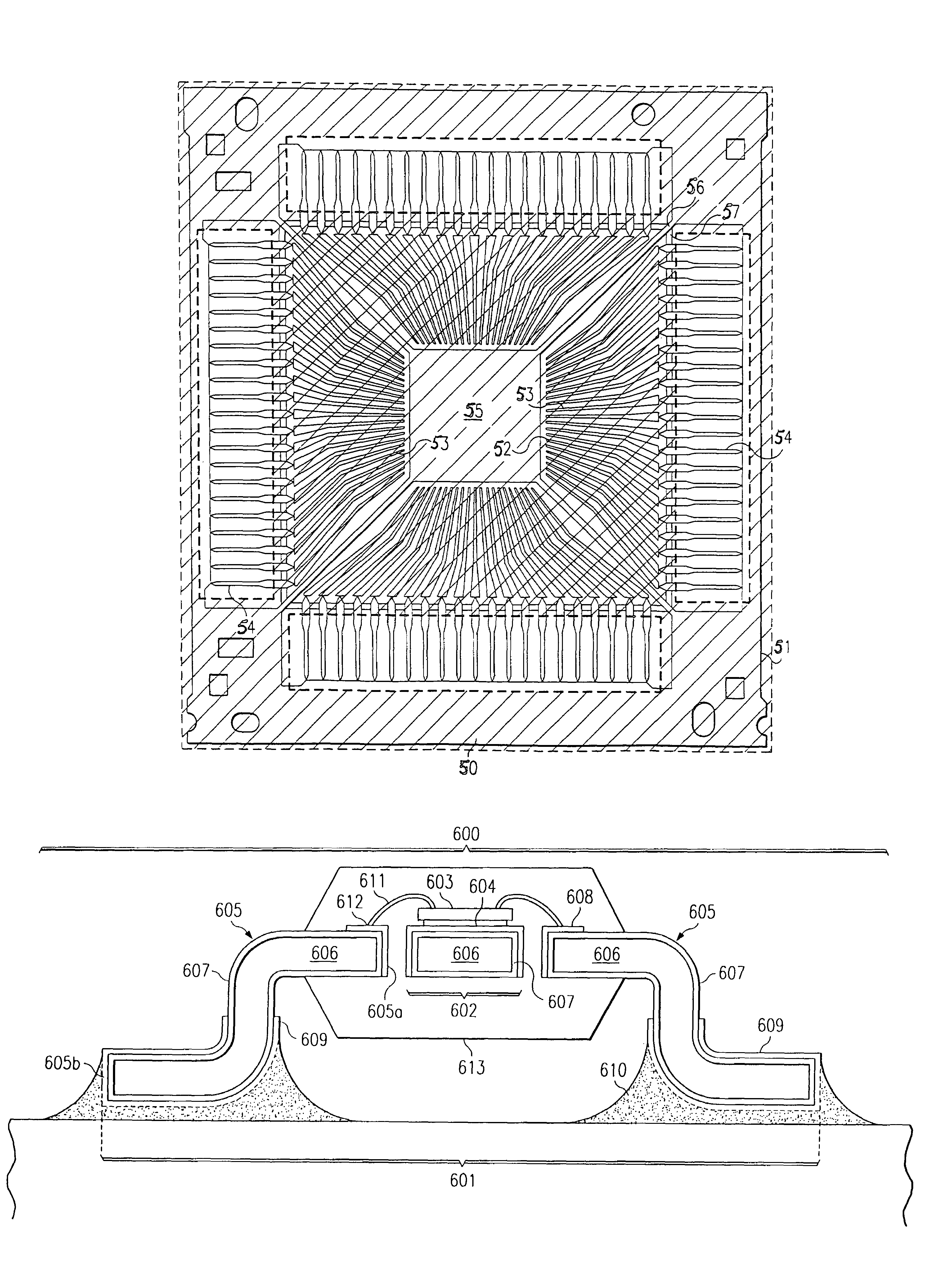
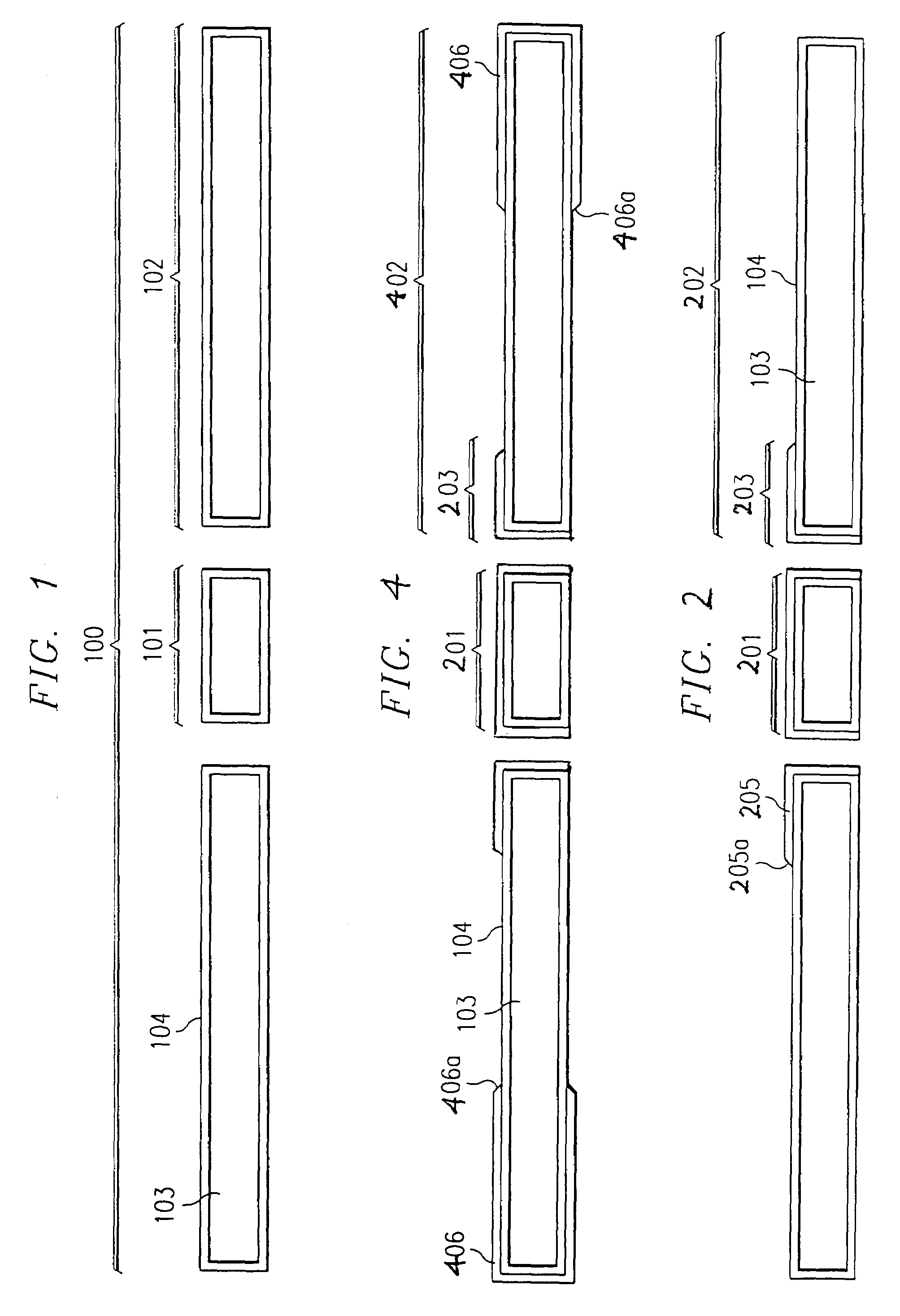
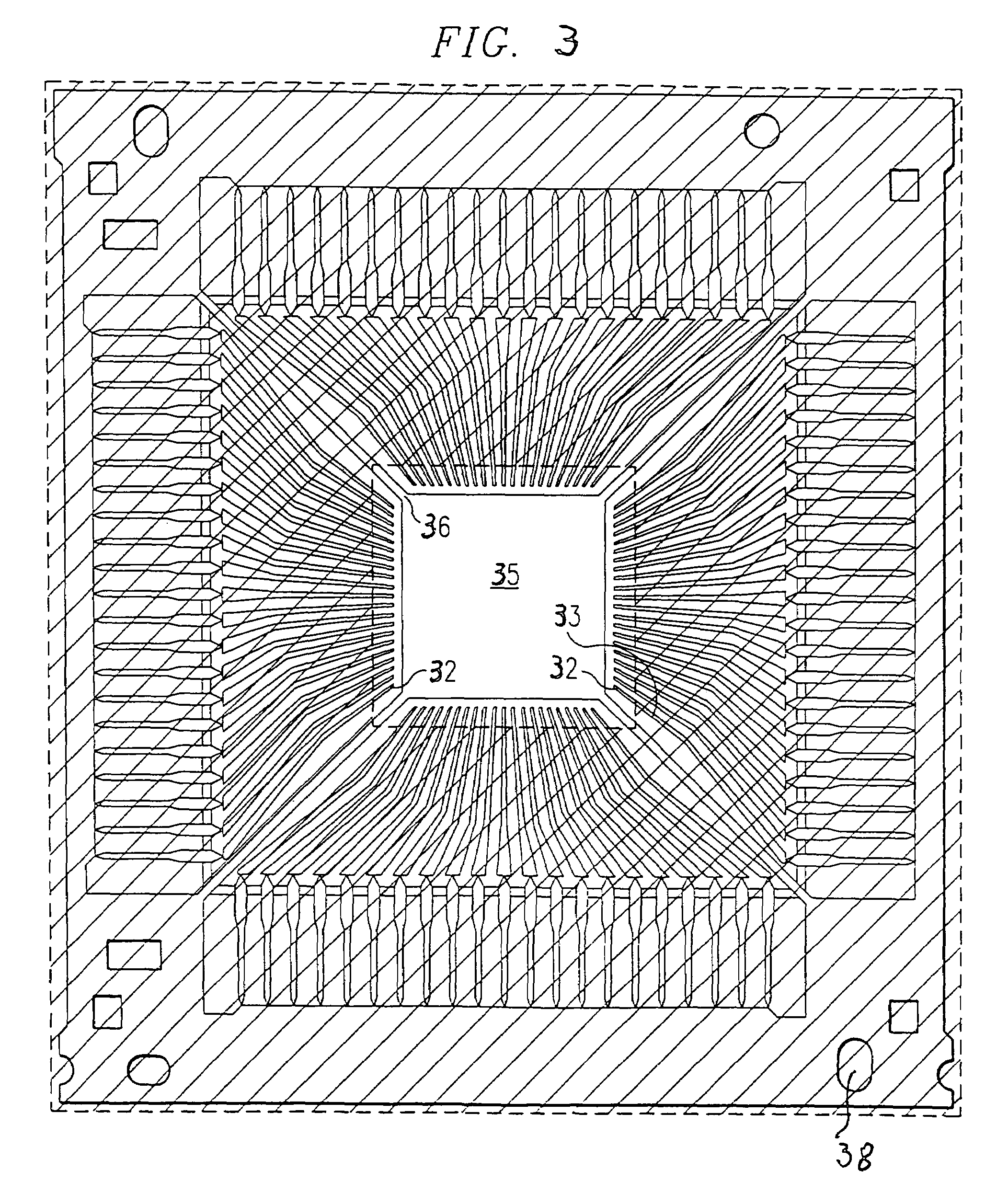
[0033]The present invention is related to the composition and sequential construction of semiconductor leadframes and to the assembly of semiconductor chips on leadframes. This assembly includes wire bonding interconnection, chip encapsulation, and the environmentally friendly process of reliable attachment of the devices to substrates using lead-free solder.

[0034]The invention reduces the cost of leadframes while the leadframe functions are maximized. The invention best applies to any leadframe and any substrate used in semiconductor tech...


PUM

PropertyMeasurementUnit
thicknessaaaaaaaaaa
thicknessaaaaaaaaaa
thicknessaaaaaaaaaa

Abstract

A leadframe for use with integrated circuit chips comprising a base metal having a plated layer of nickel fully covering the base metal; a plated layer of pure tin on the nickel layer, selectively covering areas of the leadframe intended for attachment to other parts; and a plated layer of palladium on said nickel layer, selectively covering areas of said Leadframe intended for bonding wire attachment.

Description

[0001]This application is a continuation of application Ser. No. 10 / 061,823 filed Feb. 1, 2002 now U.S. Pat. No. 6,713,852.FIELD OF THE INVENTION[0002]The present invention is related in general to the field of semiconductor devices and processes and more specifically to the materials and fabrication of leadframes for integrated circuit devices.DESCRIPTION OF THE RELATED ART[0003]The leadframe for semiconductor devices was invented (U.S. Pat. Nos. 3,716,764 and 4,034,027) to serve several needs of semiconductor devices and their operation simultaneously: First of all, the leadframe provides a stable support pad for firmly positioning the semiconductor chip, usually an integrated circuit (IC) chip. Since the leadframe including the pads is made of electrically conductive material, the pad may be biased, when needed, to any electrical potential required by the network involving the semiconductor device, especially the ground potential.[0004]Secondly, the leadframe offers a plurality o...

Claims


Application Information

Patent Timeline
Patent Type & Authority Patents(United States)
IPC IPC(8): H01L21/50H01L23/495H05K3/34
CPCH01L23/49582H05K3/3426H01L24/48H01L24/45H01L2924/15747H01L2924/01028H01L2924/01014H01L2924/01045H01L2924/01033H01L2924/01006H01L2924/14H01L2924/10329H01L2924/10271H01L2924/10253H01L2924/014H01L2924/01082H01L2224/32245H01L2224/45124H01L2224/45144H01L2224/45147H01L2224/48091H01L2224/48247H01L2224/48599H01L2224/48699H01L2224/73265H01L2224/85439H01L2224/85464H01L2924/01013H01L2924/01029H01L2924/01032H01L2924/01046H01L2924/01047H01L2924/0105H01L2924/01078H01L2924/01079H01L2924/00014H01L2924/00012H01L2924/00H01L2924/181H01L2224/48639H01L2224/48839H01L2224/48864H01L2224/48664H01L2224/48739H01L2224/48764H01L24/73Y02P70/50
Inventor ABBOTT, DONALD C.ROMM, DOUGLAS W.
Owner TEXAS INSTR INC
Why Eureka
Try Eureka