NAND string wordline delay reduction

a technology of nand memory device and word line, applied in the field of memory device, can solve the problems of reducing the overall selection time, reducing the selection delay of word lines, and causing voltage spikes within the word line, so as to reduce the average feature size, reduce the selection delay of word lines, and reduce the effect of resistan

Active Publication Date: 2006-06-20
MICRON TECH INC
View PDF7 Cites 53 Cited by
  • Summary
  • Abstract
  • Description
  • Claims
  • Application Information

AI Technical Summary

Benefits of technology

[0010]The various embodiments relate to NAND flash memory strings, memory arrays, and memory devices that utilize capacitive coupling between word lines to reduce word line selection delay. As stated above, as memory devices become denser and average feature sizes reduced, the word lines can have a relatively large resistance due to reduced the cross-sectional area of the word lines and / or their increased run lengths. This increased resistance has the effect of increasing the RC time constant of the word lines, thus increasing the time for voltage changes to propagate down a given word line. In addition, the reduced feature sizes and increased memory array density place the word lines in close proximity to each other, increasing the capacitive coupling of each of the word lines to each other. This increased word line to word line capacitive coupling generate voltage spikes within the word lines left at lower voltages when their adjacent neighbors are driven higher which must be damped out before access of the selected memory cells. Embodiments of the present invention take advantage of the asymmetric nature of the word line to word line capacitive coupling to reduce word line selection delay by driving the adjacent word lines to a higher initial voltage and then reducing it. As the capacitive coupling in between the NAND word lines produces a larger effect when the voltages are being lowered, this has the effect of damping out the voltage initially induced by the rising voltages on the adjacent word lines, reducing the overall selection time. In one embodiment, only the word lines of a NAND flash memory device that are immediately adjacent to a word line driven at a lower voltage are initially driven higher and then reduced to their target voltage to damp the capacitively coupled voltage on the lower voltage word line. In another embodiment of the present invention, all the adjacent word lines of a selected area of a NAND flash memory device are initially driven higher and then reduced to their target voltage to damp the capacitively coupled voltage on another adjacent word line driven to a lower voltage level.

Problems solved by technology

There is usually a delay in the selection of the word lines.
This increases the capacitive coupling of each of the parallel word lines to their immediately adjacent word lines and can induce voltage spikes within the word line due to word line capacitive coupling to the adjacent word lines.
As the capacitive coupling in between the NAND word lines produces a larger effect when the voltages are being lowered, this has the effect of damping out the voltage initially induced by the rising voltages on the adjacent word lines, reducing the overall selection time.

Method used


Image

  • NAND string wordline delay reduction
  • NAND string wordline delay reduction
  • NAND string wordline delay reduction

Examples


Embodiment Construction

[0019]In the following detailed description of the invention, reference is made to the accompanying drawings that form a part hereof, and in which is shown, by way of illustration, specific embodiments in which the invention may be practiced. In the drawings, like numerals describe substantially similar components throughout the several views. These embodiments are described in sufficient detail to enable those skilled in the art to practice the invention. Other embodiments may be utilized and structural, logical, and electrical changes may be made without departing from the scope of the present invention. The following detailed description is, therefore, not to be taken in a limiting sense, and the scope of the present invention is defined only by the appended claims and equivalents thereof.

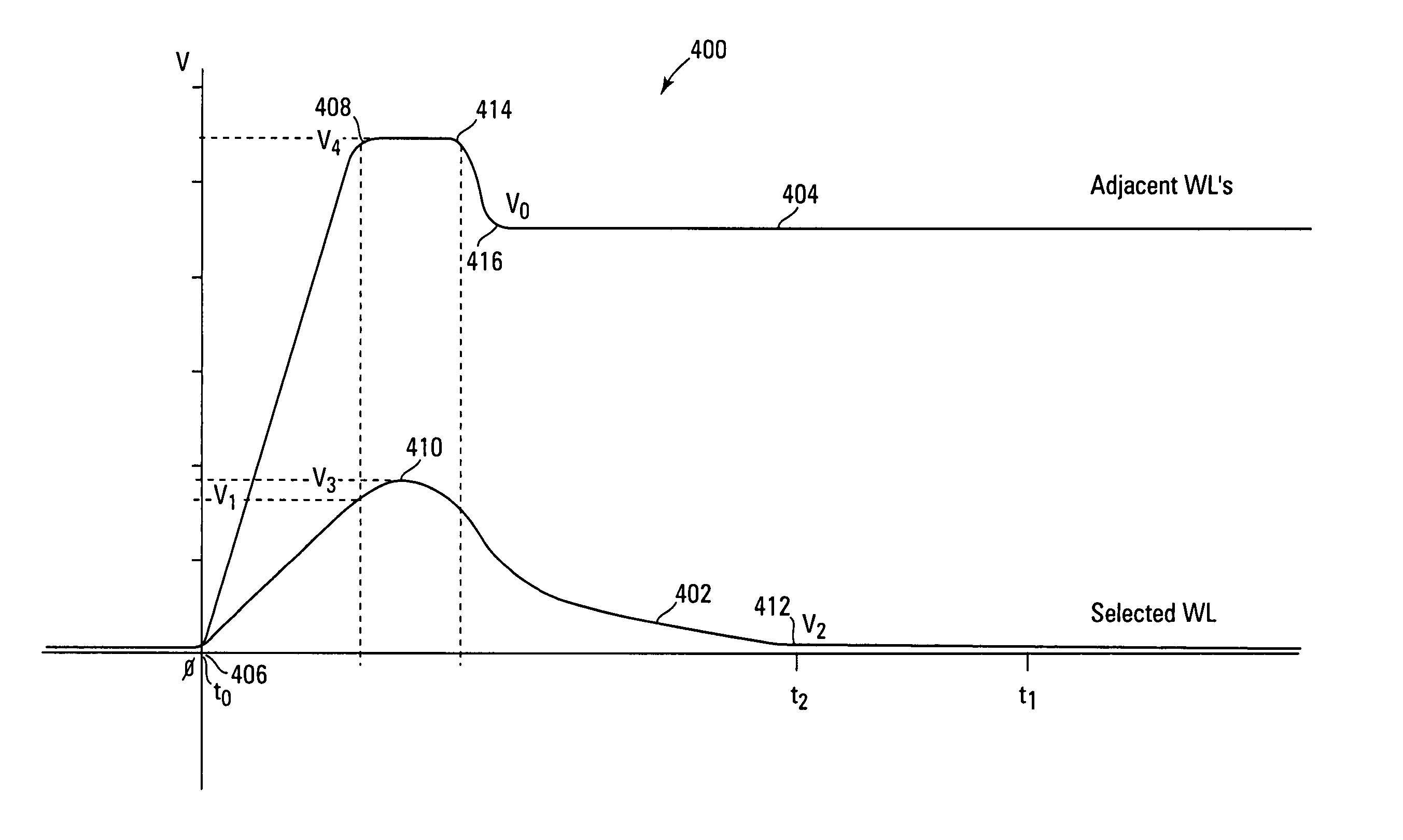
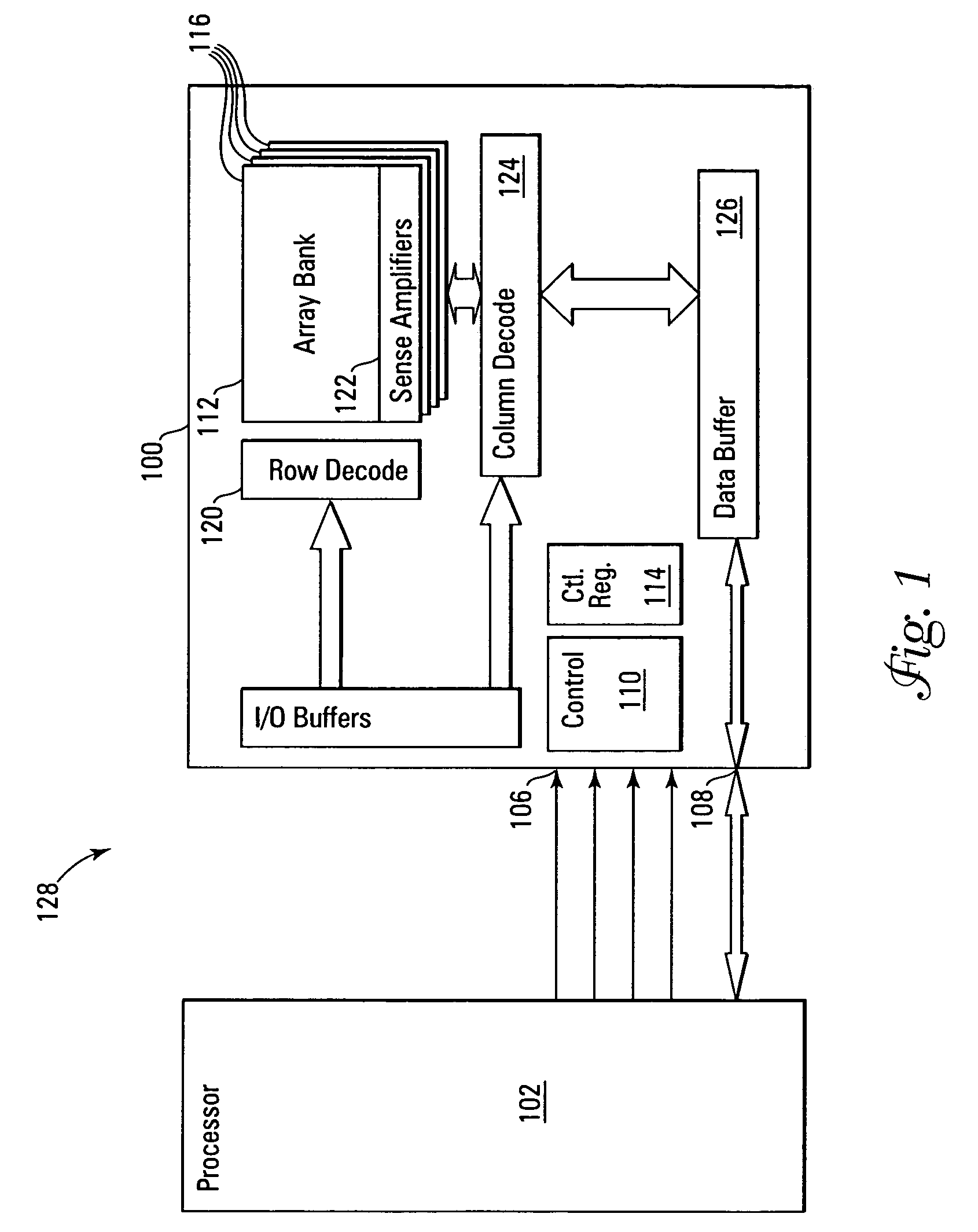
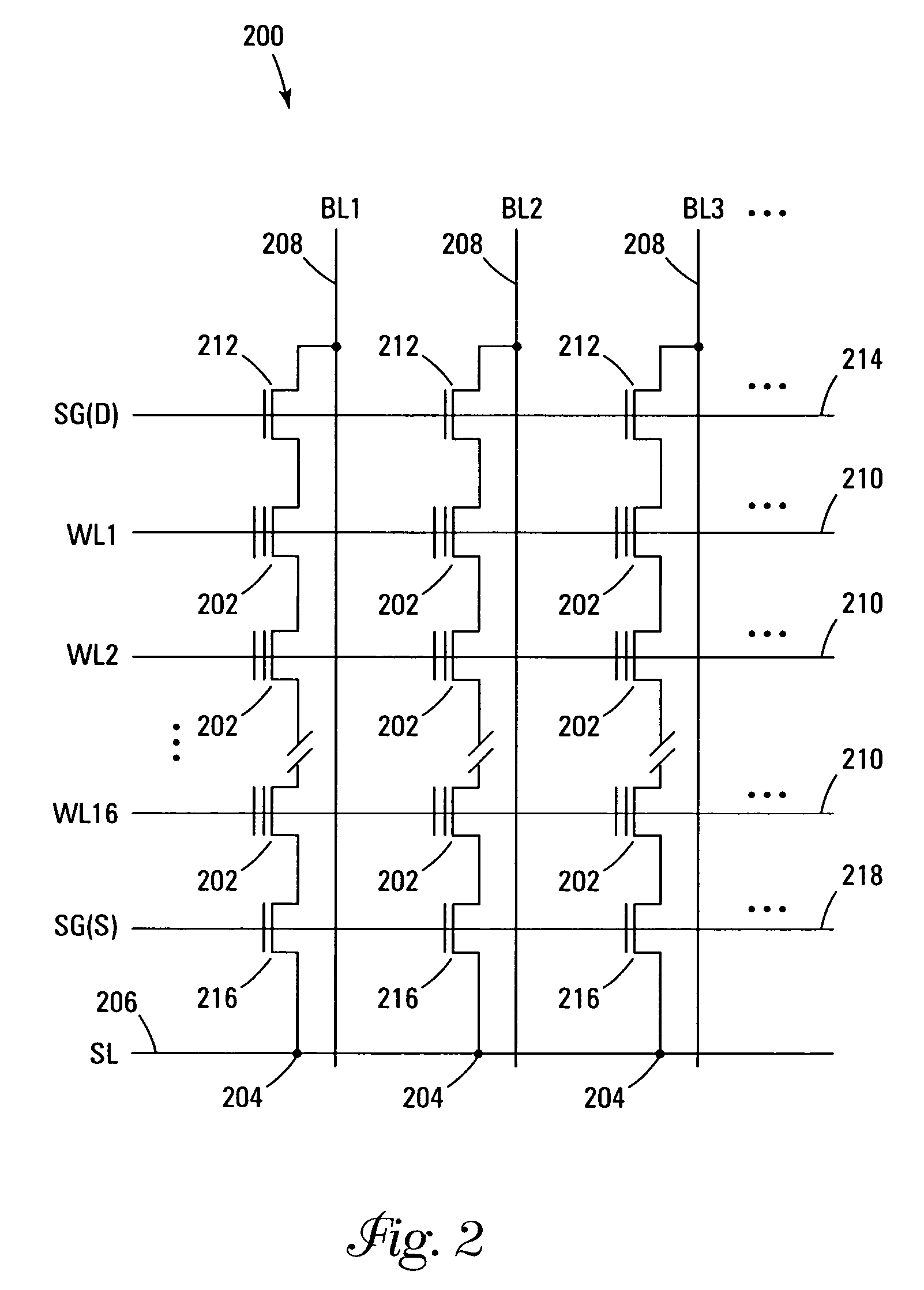
[0020]FIG. 1 shows a simplified diagram of a system 128 incorporating a NAND architecture Flash memory 100 embodiment of the present invention connected to a host 102, which is typically a proce...


PUM


Abstract

An improved NAND Flash memory and word line selection method has been described, that takes advantage of the asymmetric nature of the word line to word line capacitive coupling to reduce word line selection delay by driving the adjacent word lines to a higher initial voltage and then reducing it to the final target voltage. As the capacitive coupling in between the NAND word lines is a larger effect when the voltages are being lowered, this has the effect of damping out the voltage initially induced in the lower voltage word line by the rising voltages on the adjacent word lines, reducing the overall selection time.

Description

TECHNICAL FIELD OF THE INVENTION[0001]The present invention relates generally to memory devices and in particular the present invention relates to delay reduction in word lines of NAND memory devices.BACKGROUND OF THE INVENTION[0002]Memory devices are typically provided as internal storage areas in computers. The term memory identifies data storage that comes in the form of integrated circuit chips. In general, memory devices contain an array of memory cells for storing data, and row and column decoder circuits coupled to the array of memory cells for accessing the array of memory cells in response to an external address.[0003]One type of memory is a non-volatile memory known as flash memory. A flash memory is a type of EEPROM (electrically-erasable programmable read-only memory) that can be erased and reprogrammed in blocks. Many modern personal computers (PCs) have their BIOS stored on a flash memory chip so that it can easily be updated if necessary. Such a BIOS is sometimes call...

Claims


Application Information

Patent Timeline
Patent Type & Authority Patents(United States)
IPC IPC(8): G11C16/04
CPCG11C16/26G11C16/0483
Inventor ROOHPARVAR, FRANKIE F.
Owner MICRON TECH INC
Why Eureka
Try Eureka