Dispersion compensation device

a dispersion compensation and dispersion compensation technology, applied in multiplex communication, cladded optical fibre, instruments, etc., can solve the problems of high loss loss through waveguides, and it is difficult to apply the dispersion compensation device of such a high loss to ultrafast and large-capacity optical communication using a broad spectral band, and achieve low loss dispersion compensation and reliable dispersion compensation

Inactive Publication Date: 2006-06-20
FUJIKURA LTD
View PDF6 Cites 37 Cited by
  • Summary
  • Abstract
  • Description
  • Claims
  • Application Information

AI Technical Summary

Benefits of technology

[0011]Therefore, this invention aims to provide a new dispersion compensation device of a low loss and capable of realizing a higher transmission rate for the optical communication utilizing ultrashort optical pulses.
[0030]As described above, according to the present invention, since the photonic crystal part for providing a chromatic dispersion and the waveguide for conducting the light is prepared separately, it is possible to provide a low loss dispersion compensation device where a free design of the cross-section area of the waveguide can be practiced, the optical pulses can take into the device with keeping the loss to a minimum, and thus the dispersion compensation can make reliably.

Problems solved by technology

When optical pulses are launched into such a waveguide having a small cross-sectional area, loss through the waveguide will be very large.
It is hardly possible to apply the dispersion compensation device of such a high loss to the ultrafast and large capacity optical communication utilizing a broad spectral band.

Method used


Image

  • Dispersion compensation device
  • Dispersion compensation device
  • Dispersion compensation device

Examples


example 1

(1) Modified Example 1 of the Photonic Crystal Layer

[0113]A modified configuration example of the photonic crystal layer 4 is described with reference to FIGS. 5A, 5B.

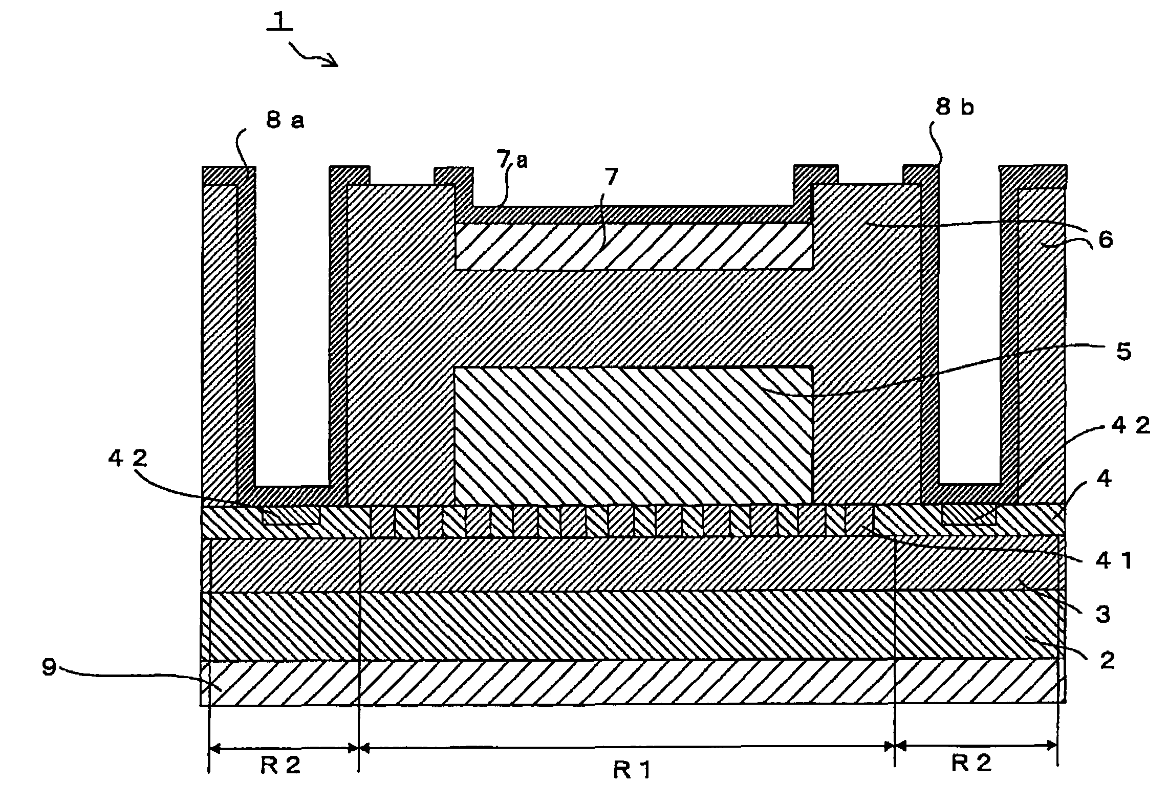
[0114]In the above described embodiment, the photonic crystal layer 4 is composed of the photonic crystal region R1 and extended regions R2, the photonic crystal region R1 being prepared by providing a plural number of plane-shaped holes 41 to the matrix material which is made of Si, and then filling up the holes 41 with SiO2 film of which dielectric constant is different from that of the matrix material, and the extended regions being located at both sides of the photonic crystal region R1 and being not provided with the hole 41. In this modified example, further by providing the barrier regions to inhibit or to restrain the propagation of the light and which are formed by a material the refractive index of which is smaller than Si at both side of the photonic crystal region R1, it is possible to transmit the light tr...

example 2

(2) Modified Example 2 of the Photonic Crystal Layer.

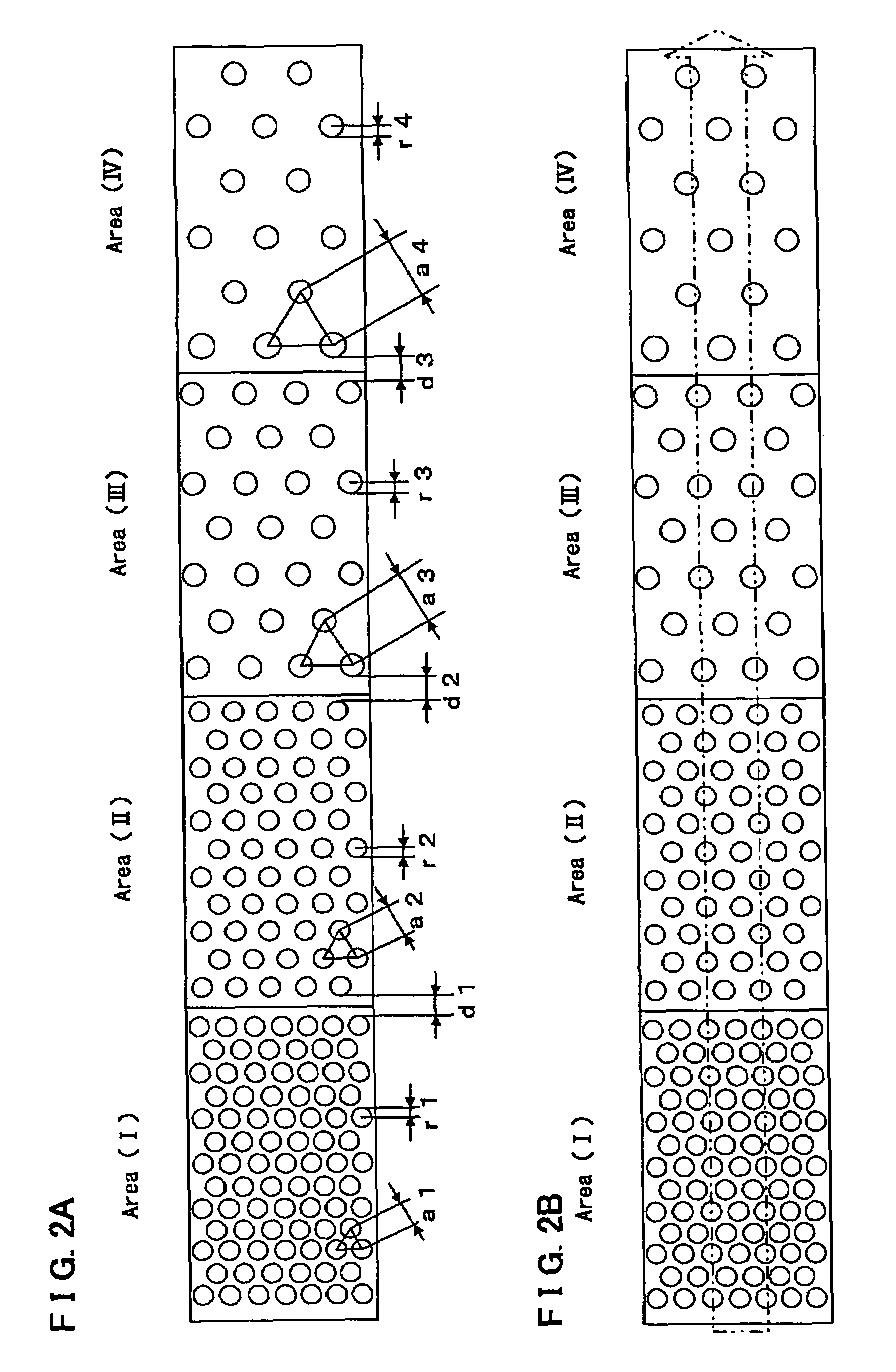
[0119]Another modified configuration example of the photonic crystal layer 4 is described with reference to FIG. 6. In this example, the barrier areas as mentioned above can be realized by forming holes 41 in a different condition from that of above mentioned embodiment in the photonic crystal area R1.

[0120]FIG. 6 is an illustrative view for another modified construction example of the photonic crystal layer 4 which has holes 41 formed in the photonic crystal region R1 with a modified condition.

[0121]An interval (pitch) between holes 41 in each area is described using FIG. 6. Incidentally, we suppose that we explain the photonic crystal where the photonic band region is laid on the area (I) or area (II) as the lower-branch photonic band region.

[0122]Assuming that the interval (pitch) between holes 41 in the photonic crystal region R1 is aR1, the interval (pitch) between holes 41 in the barrier region is aR2, the center-to-center i...


PUM


Abstract

A dispersion compensation device for compensating chromatic dispersion of optical pulses launched from the exterior is disclosed. The device comprises a waveguide and a photonic crystal part, the waveguide comprising a core part for guiding the optical pulse from an input end to an output end and a clad part consisting of a first clad layer and a second clad layer, the photonic crystal part providing a chromatic dispersion variation of a proper dispersion characteristic to the optical pulses guided through the waveguide, the chromatic dispersion variation having an absolute value of the variation and a positive or negative sign, wherein the photonic crystal part is layered onto the first clad layer, the core part is layered onto the photonic crystal part, and the second clad part is formed so that a portion of which is layered onto the photonic crystal part and a remaining part of which covers the exposed surface of the core part.

Description

TECHNICAL FIELD[0001]This invention relates to a dispersion compensation device, particularly, this invention relates to a low-loss dispersion compensation device which is provided with a photonic crystal region and a core region for leading light, wherein the photonic crystal region and the core region are separately formed.RELATED ARTS[0002]In recent years, long-haul data communication has been performed through optical fibers, and the transmission rate of data has risen drastically from the past. With respect to the data communication through such optical fibers, communication using ultrashort optical pulses at a rate of 160 Gbit / s or more, which rate is extremely higher than the rate presently used, is now under investigation.[0003]When performing the data communication, usually, the problems about crosstalk and transmission error would come up. The higher transmission velocity of the data, the narrower temporal width of individual optical pulse and time interval between adjacen...

Claims


Application Information

Patent Timeline
Patent Type & Authority Patents(United States)
IPC IPC(8): G02B6/02G02B6/10G02B6/44H04J14/02
CPCB82Y20/00G02B6/29394G02B6/1225
Inventor OGAWA, KENSUKETAN, YONG-TSONG
Owner FUJIKURA LTD
Why Eureka
Try Eureka